

Philips 83c576, 87576 DATASHEETS

INTEGRATED CIRCUITS
83C576/87C576
80C51 8-bit microcontroller family
8K/256 OTP/ROM, 6 channel 10-bit A/D,
4 comparators, failure detect circuitry, watchdog timer
Product specification
Supersedes data of 1998 Jan 06
IC20 Data Handbook
1998 Jun 04
Philips Semiconductors Product specification
80C51 8-bit microcontroller family
8K/256 OTP/ROM, 6 channel 10-bit A/D, 4 comparators,
failure detect circuitry, watchdog timer
83C576/87C576
FEA TURES
•80C51 based architecture
– 8k × 8 ROM (83C576)
– 8k × 8 EPROM (87C576)
– 256 × 8 RAM
– 10-bit, 6 channel A/D
– Three 16-bit counter/timers
– 2 PWM outputs
– Programmable Counter Array
– Universal Peripheral Interface
– Enhanced UART
– Oscillator fail detect
– Low active reset
– 4 analog comparators
– Watchdog timer
– Low V
– Power-on detect
CC
detect
•Memory addressing capability
– 64k ROM and 64k RAM
•Power control modes:
– Idle mode
– Power-down mode
•CMOS and TTL compatible
•6 to 16MHz
•Extended temperature ranges
•OTP available
•That can be programmed in circuit
•Software Reset
•15 source, 2 level interrupt structure
•Lower EMI noise
•Programmable I/O pins
•Serial on-board programming
•Schmitt trigger inputs on Port 1
DESCRIPTION
The Philips 83C576/87C576 is a high-performance microcontroller
fabricated with Philips high-density CMOS technology. The Philips
CMOS technology combines the high speed and density
characteristics of HMOS with the low power attributes of CMOS.
Philips epitaxial substrate minimizes latch-up sensitivity.
The 8XC576 contains an 8k × 8 ROM (83C576) EPROM (87C576),
a 256 × 8 RAM, 32 I/O lines, three 16-bit counter/timers, a
Programmable Counter Array (PCA), a 10-bit, 6 channel A/D,
2 PWM outputs, an 8-bit UPI interface, a fifteen-source, two-priority
level nested interrupt structure, an enhanced UART, four analog
comparators, power-fail detect and oscillator fail detect circuits, and
on-chip oscillator and clock circuits.
In addition, the 8XC576 has a low active reset, and a software reset.
There is also a fully configurable watchdog timer, and internal power
on clear circuit. The part includes idle mode and power-down mode
states for reduced power consumption.
ORDERING INFORMATION
ROM EPROM
P83C576EBPN P87C576EBPN OTP 0 to +70, 40-Pin Plastic Dual In-line Package 16 SOT129-1
P83C576EBAA P87C576EBAA OTP 0 to +70, 44-Pin Plastic Leaded Chip Carrier 16 SOT187-2
P83C576EBBB P87C576EBBB OTP 0 to +70, 44-Pin Plastic Quad Flat Pack 16 SOT307-2
P83C576EFPN P87C576EBPN OTP –40 to +85, 40-Pin Plastic Dual In-line Package 16 SOT129-1
P83C576EFAA P87C576EFAA OTP –40 to +85, 44-Pin Plastic Leaded Chip Carrier 16 SOT187-2
P83C576EFBB P87C576EFBB OTP –40 to +85, 44-Pin Plastic Quad Flat Pack 16 SOT307-2
P83C576EHPN P87C576EHPN OTP –40 to +125, 40-Pin Plastic Dual In-line Package 16 SOT129-1
P83C576EHAA P87C576EHAA OTP –40 to +125, 44-Pin Plastic Leaded Chip Carrier 16 SOT187-2
P83C576EHBB P87C576EHBB OTP –40 to +125, 44-Pin Plastic Quad Flat Pack 16 SOT307-2
NOTE:
1. OTP - One Time Programmable EPROM.
1
TEMPERATURE RANGE °C AND PACKAGE
FREQ
(MHz)
DRAWING
NUMBER
1998 Jun 04 853-2067 19495
2
Philips Semiconductors Product specification
80C51 8-bit microcontroller family
8K/256 OTP/ROM, 6 channel 10-bit A/D, 4 comparators,
failure detect circuitry, watchdog timer
BLOCK DIAGRAM
P0.0-P0.7 P2.0-P2.7
83C576/87C576
V
CC
PSEN
V
SS
REGISTER
WATCHDOG
ALE
EA
RST
TIMING
CONTROL
XTAL1 XTAL2
UPI
CONTROL
LOW
VOLTAGE
DETECT
AB
RAM ADDR
REGISTER
B
TIMER
AND
INSTRUCTION
PD
OSCILLATOR
B
A
REGISTER
CLK AND OSC
POWER
ON
DETECT
RAM
FAILURE
DETECT
ACC
TMP2
DRIVERS
PSW
PORT 1
LATCH
PORT 1
DRIVERS
PORT 0
PORT 0
LATCH
ALU
TMP1
TIMERS
10-BIT
ANALOG TO DIGITAL
CONVERTER
PORT 2
DRIVERS
PORT 2
LATCH
SFRs
PCA
STACK
POINTER
PORT 3
LATCH
PORT 3
DRIVERS
ROM/
EPROM
PROGRAM
ADDRESS
REGISTER
BUFFER
PC
INCRE-
MENTER
PROGRAM
COUNTER
DPTR
COMPARATOR
BLOCK
PWM
1998 Jun 04
P1.0-P1.5
+AV
CC
P3.0-P3.7
–AV
SS
SU00255B
3
Philips Semiconductors Product specification
80C51 8-bit microcontroller family
8K/256 OTP/ROM, 6 channel 10-bit A/D, 4 comparators,
failure detect circuitry, watchdog timer
LOGIC SYMBOL
V
V
SS
CC
XTAL1
XTAL2
ADDRESS AND
DATA BUS
PORT 0
83C576/87C576
DB0
DB1
DB2
DB3
DB4
DB5
DB6
DB7
CMP3+
CMP2+
CMP1+
CMPR–
CMP0+
CMP0–
PIN CONFIGURA TIONS
44-pin Plastic Quad Flat Pack
44 34
1
PQFP
11
12 22
Pin Function
1 ADIN3/P1.3
2 ADIN4/P1.4
3 ADIN5/P1.5
4 RST
5 RxD/P3.0
6 NC*
7 TXD/P3.1
0/P3.2/CMP3+
8 INT
1/P3.3/CMP2+
9 INT
10 T0/P3.4/CMP1+
11 T1/P3.5/CMPR–
/P3.6/CMP0+
12 WR
13 RD
/P3.7CMP0–
14 XTAL2
15 XTAL1
* NO INTERNAL CONNECTION
Pin Function
16 V
SS
17 NC*
18 P2.0/A8/CEX0/CMP0
19 P2.1/A9/CEX1/CMP1
20 P2.2/A10/CEX2/CMP2
21 P2.3/A11/CEX3/CMP3
22 P2.4/A12/T2EX/A0
23 P2.5/A13/T2/CS
24 P2.6/A14/CEX4/PWM0
25 P2.7/A15/PWM1/ECI
26 PSEN
27 ALE/PROG
28 NC*
/V
29 EA
PP
30 P0.7/AD7/DB7
EA/V
PSEN
ALE/PROG
RxD
TxD
INT0
INT1
T0
T1
WR
RD
SECONDARY FUNCTIONS
33
23
Pin Function
31 P0.6/AD6/DB6
32 P0.5/AD5/DB5
33 P0.4/AD4/DB4
34 P0.3/AD3/DB3
35 P0.2/AD2/DB2
36 P0.1/AD1/DB1
37 P0.0/AD0/DB0
38 V
39 NC*
40 +V
41 –V
42 ADIN0/P1.0
43 ADIN1/P1.1
44 ADIN2/P1.2
RST
PP
PORT 3
CC
REF
REF
/AV
CC
/AV
SS
SU00253B
ADIN0
ADIN1
PORT 1PORT 2
SECONDARY FUNCTIONS
ADDRESS BUS
ADIN2
ADIN3
ADIN4
ADIN5
PWM1/ECI
CEX4/PWM0
T2/CS#
T2EX/A0
CEX3/CMP3
CEX2/CMP2
CEX1/CMP1
CEX0/CMP0
SU00254A
Plastic Leaded Chip Carrier
6140
7
LCC
17
18 28
Pin Function
1 NC*
2+V
/AV
REF
3–V
4 ADIN0/P1.0
5 ADIN1/P1.1
6 ADIN2/P1.2
7 ADIN3/P1.3
8 ADIN4/P1.4
9 ADIN5/P1.5
10 RST
11 RxD/P3.0
12 NC*
13 TxD/P3.1
14 INT
15 INT
* NO INTERNAL CONNECTION
CC
/AV
REF
SS
0/P3.2/CMP3+
1/P3.3/CMP2+
Pin Function
16 T0/P3.4/CMP1+
17 T1/P3.5/CMPR–
/P3.6/CMP0+
18 WR
19 RD
/P3.7/CMP0–
20 XTAL2
21 XTAL1
22 V
SS
23 NC*
24 P2.0/A8/CEX0/CMP0
25 P2.1/A9/CEX1/CMP1
26 P2.2/A10/CEX2/CMP2
27 P2.3/A11/CEX3/CMP3
28 P2.4/A12/T2EX/A0
29 P2.5/A13/T2/CS
30 P2.6/A14/CEX4/PWM0
39
29
Pin Function
31 P2.7/A15/PWM1/ECI
32 PSEN
33 ALE/PROG
34 NC*
/V
35 EA
PP
36 P0.7/AD7/DB7
37 P0.6/AD6/DB6
38 P0.5/AD5/DB5
39 P0.4/AD4/DB4
40 P0.3/AD3/DB3
41 P0.2/AD2/DB2
42 P0.1/AD1/DB1
43 P0.0/AD0/DB0
44 V
CC
SU00252A
1998 Jun 04
4

Philips Semiconductors Product specification
80C51 8-bit microcontroller family
8K/256 OTP/ROM, 6 channel 10-bit A/D, 4 comparators,
failure detect circuitry, watchdog timer
PIN DESCRIPTIONS
PIN NUMBER
MNEMONIC
V
SS
V
CC
P0.0-0.7 39-32 43-36 37-30 I/O Port 0: Port 0 is a bidirectional I/O port. Port 0 is also the multiplexed low-order address and
P1.0-P1.5 3-8 5-9 42-44
P2.0-P2.7 21-28 24-31 18-25 I/O Port 2: Port 2 is an 8-bit bidirectional I/O port. Port 2 emits the high-order address byte
DIP LCC QFP TYPE NAME AND FUNCTION
20 22 16 I Ground: 0V reference.
40 44 38 I Power Supply: This is the power supply voltage for normal, idle, and power-down operation.
data bus during accesses to external program and data memory (see Note 5). In this
application, it uses strong internal pull-ups when emitting 1s. Port 0 also receives code bytes
during parallel EPROM programming and outputs code bytes during verification. External
pull-ups are required during program verification. During reset, the port register is loaded
with 1’s. Port 0 has 4 output modes selected on a per bit basis by writing to the P0M1 and
P0M2 Special Function Registers as follows:
P0M1.x P0M2.x Mode Description
0 0 Open drain (default). See Note 1.
0 1 W eak pullup. See Note 2.
1 0 High impedance. See Note 3.
1 1 Push-pull. See Note 4.
Port 0 is also the data I/O port for the Universal Peripheral Interface (UPI). When the UPI is
enabled, port 0 must be configured as High-Z by the user. Input/Output through P0 is
controlled by pin CS
I/O Port 1: Port 1 is a 6-bit bidirectional I/O port with Schmitt trigger inputs. Port 1 receives the control
1-3
3 4 42 I/O P1.0/ADIN0
4 5 43 I/O P1.1/ADIN1
5 6 44 I/O P1.2/ADIN2
6 7 1 I/O P1.3/ADIN3
7 8 2 I/O P1.4/ADIN4
8 9 3 I/O P1.5/ADIN5
21 24 18 P2.0 CEX0 PCA module 0 external I/O
22 25 19 P2.1 CEX1 PCA module 1 external I/O
23 26 20 P2.2 CEX2 PCA module 2 external I/O
24 27 21 P2.3 CEX3 PCA module 3 external I/O
25 28 22 P2.4 T2EX timer 2 capture input
26 29 23 P2.5 T2 timer 2 external I/O — clock-out (programmable)
27 30 24 P2.6 CEX4 PCA module 4 external I/O
28 31 25 P2.7 ECI PCA count input
signals during program memory verification and parallel EPROM programming. During reset, port
1 is configured as a high impedance analog input port. Digital push-pull outputs are enabled by
writing 1’s to the P1M1 register. The programmer must take care to prevent digital outputs from
switching while an A/D conversion is in progress. Port 1 has 3 output modes selected on a per bit
basis by writing to the P1M1 and P1M2 special function registers as follows:
P1M1.X P1M2.X Mode Description
0 0 A/D only. (High impedance)
0 1 Digital input only. High impedance (default).
1 X Push-pull.
Port 1 pins also serve alternate functions as follows:
during accesses to external program and data memory that use 16-bit addresses (MOVX
@DPTR) (see Note 5). In this application, it uses strong internal pull-ups when emitting 1s.
Port 2 receives the high-order address byte during program verification and parallel EPROM
programming. During reset, the port 2 pullups are turned on synchronously, and the port
register is loaded with 1’s. Port 2 has the following output modes which can be selected on a
per bit basis by writing to P2M1 and P2M0:
P2M1.X P2M2.X Mode Description
0 0 Open drain. See Note 1.
0 1 W eak pullup (default). See Note 2.
1 0 High impedance. See Note 3.
1 1 Push-pull. See Note 4.
Port 2 pins serve alternate functions as follows:
, WR, RD, and A0. Output is push-pull when enabled.
CMP0 comparator 0 output
CMP1 comparator 1 output
CMP2 comparator 2 output
CMP3 comparator 3 output
A0 UPI address input
CS UPI chip select input
PWM0 Pulse width modulator 0 output
PWM1 Pulse width modulator 1 output
83C576/87C576
1998 Jun 04
5

Philips Semiconductors Product specification
80C51 8-bit microcontroller family
8K/256 OTP/ROM, 6 channel 10-bit A/D, 4 comparators,
failure detect circuitry, watchdog timer
PIN DESCRIPTIONS (Continued)
PIN NUMBER
MNEMONIC DIP LCC QFP TYPE NAME AND FUNCTION
+V
/AV
REF
–V
/AV
REF
P3.0-P3.7 10-17 11,
RST 9 10 4 I Reset: A low on this pin synchronously resets all port pins to a high state. The pin must be
ALE/PROG 30 33 27 I/O Address Latch Enable/Program Pulse: Output pulse for latching the low byte of the address
PSEN 29 32 26 O Program Store Enable: The read strobe to external program memory. When the device is
EA/V
PP
XTAL1 19 21 15 I Crystal 1: Input to the inverting oscillator amplifier and input to the internal clock generator
XTAL2 18 20 14 O Crystal 2: Output from the inverting oscillator amplifier.
NOTES:
1. When Open Drain mode is selected, ports 0 and 2 have weak pulldowns to guarantee positive leakage current (see DC electrical
characteristic I
2. When Weak Pullup mode is selected, ports bits that have 1’s written to them can be used as inputs but will source current when externally
pulled low (see DC electrical characteristic IIL).
3. When High Impedance mode is selected, all pullups and pulldowns are turned off. The only current sourced or sunk by the pin is the
parasitic leakage current (see DC electrical characteristic I
4. When Push-Pull mode is selected, strong pullups are on continuously when emitting 1’s (see DC electrical characteristic V
5. When Open-Drain, Weak Pull-up, or Push-pull mode is selected.
1 2 40 I A/D positive power supply
CC
2 3 41 I A/D 0V reference
SS
I/O Port 3: Port 3 is an 8-bit bidirectional I/O port. Port 3 pins that have 1s written to them can
13-195,7-13
be used as inputs but will source current when externally pulled low (see DC Electrical
Characteristics: I
high until written to by software. Port 3 has the following output modes which can be
). During reset all pins will be synchronously driven high and will remain
IL
selected on a per bit basis by writing to P3M1 and P3M2:
P3M1.X P3M2.X Mode Description
0 0 Open drain. See Note 1.
0 1 W eak pullup (default). See Note 2.
1 0 High impedance. See Note 3.
1 1 Push-pull. See Note 4.
Port 3 pins serve alternate functions as follows:
10 11 5 I P3.0 RxD Serial receive port
11 13 7 O P3.1 TxD Serial transmit port (enabled only when transmitting serial data)
12 14 8 I P3.2 INT0 External interrupt 0
CMP3+ Comparator 3 positive input
13 15 9 I P3.3 INT1 External interrupt 1
CMP2+ Comparator 2 positive input
14 16 10 I P3.4 T0 Timer/counter 0 input
CMP1+ Comparator 1 positive input
15 17 11 I P3.5 T1 Timer/counter 1 input
CMPR– Common reference to comparators 1, 2, 3
16 18 12 O P3.6 WR External data memory write strobe
CMP0+ Comparator 0 positive input
17 19 13 O P3.7 RD External data memory read strobe
CMP0– Comparator 0 negative input
held low with the oscillator running for 24 oscillator cycles to initialize the internal registers.
An internal diffused resistor to V
capacitor to V
with a slow rising input voltage.
. RST has a Schmitt trigger input stage to provide additional noise immunity
SS
permits a power on reset using only an external
CC
during an access to external memory. In normal operation, ALE is emitted at a constant rate
of 1/6 the oscillator frequency, and can be used for external timing or clocking. Note that
one ALE pulse is skipped during each access to external data memory. ALE is switched off
if the bit 0 in the AUXR register (8EH) is set. This pin is also the program pulse input
(PROG
) during parallel EPROM programming. (See also I n t e r n a l Re s e t o n pa g e 2 4. )
executing code from the external program memory, PSEN
cycle, except that two PSEN
memory. PSEN
is not activated during fetches from internal program memory.
activations are skipped during each access to external data
31 35 29 I External Access Enable/Programming Supply Voltage: EA must be externally held low
to enable the device to fetch code from external program memory locations 0000H to
1FFFH. If EA
is held high, the device executes from internal program memory unless the
program counter contains an address greater than 1FFFH. This pin also receives the
12.75V programming supply voltage (V
voltage during reset the device enters the in-circuit programming mode.
) during EPROM programming. If this pin is at V
PP
circuits.
).
IH
or ILC, as applicable.
L2
83C576/87C576
is activated twice each machine
).
OH
PP
1998 Jun 04
6
Philips Semiconductors Product specification
80C51 8-bit microcontroller family
8K/256 OTP/ROM, 6 channel 10-bit A/D, 4 comparators,
failure detect circuitry, watchdog timer
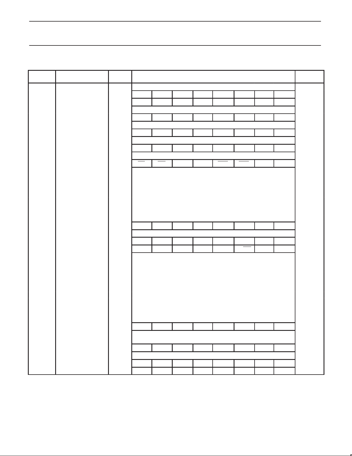
Table 1. 87C576 Special Function Registers
SYMBOL DESCRIPTION
ACC* Accumulator E0H E7 E6 E5 E4 E3 E2 E1 E0 00H
ADC0H# A/D Channel 0 MSB AAH 00H
ADC1H# A/D Channel 1 MSB ABH 00H
ADC2H# A/D Channel 2 MSB ACH 00H
ADC3H# A/D Channel 3 MSB ADH 00H
ADC4H# A/D Channel 4 MSB AEH 00H
ADC5H# A/D Channel 5 MSB AFH 00H
ADC0L# A/D Channel 0 2-LSBits 9AH 00H
ADC1L# A/D Channel 1 2-LSBits 9BH 00H
ADC2L# A/D Channel 2 2-LSBits 9CH 00H
ADC3L# A/D Channel 3 2-LSBits 9DH 00H
ADC4L# A/D Channel 4 2-LSBits 9EH 00H
ADC5L# A/D Channel 5 2-LSBits 9FH 00H
ADCON# A/D Control B1H ADF ADCE AD8M
ADCS# A/D Channel Select B2H 00H
DIRECT
ADDRESS
BIT ADDRESS, SYMBOL, OR ALTERNATIVE PORT FUNCTION
MSB LSB
AMOD1
AMOD0
ASCA2 ASCA1
83C576/87C576
RESET
VALUE
ASCA0 00H
AUXR# Auxiliary 8EH – – – – SRST TXI LO AO xxxx0000B
B* B register F0H F7 F6 F5 F4 F3 F2 F1 F0 00H
CCAP0H# Module 0 Capture High FAH xxxxxxxxB
CCAP1H# Module 1 Capture High FBH xxxxxxxxB
CCAP2H# Module 2 Capture High FCH xxxxxxxxB
CCAP3H# Module 3 Capture High FDH xxxxxxxxB
CCAP4H# Module 4 Capture High FEH xxxxxxxxB
CCAP0L# Module 0 Capture Low EAH xxxxxxxxB
CCAP1L# Module 1 Capture Low EBH xxxxxxxxB
CCAP2L# Module 2 Capture Low ECH xxxxxxxxB
CCAP3L# Module 3 Capture Low EDH xxxxxxxxB
CCAP4L# Module 4 Capture Low EEH xxxxxxxxB
CCAPM0# Module 0 Mode DAH – ECOM CAPP CAPN MAT TOG PWM ECCF x0000000B
CCAPM1# Module 1 Mode DBH – ECOM CAPP CAPN MAT TOG PWM ECCF x0000000B
CCAPM2# Module 2 Mode DCH – ECOM CAPP CAPN MAT TOG PWM ECCF x0000000B
CCAPM3# Module 3 Mode DDH – ECOM CAPP CAPN MAT TOG PWM ECCF x0000000B
CCAPM4# Module 4 Mode DEH – ECOM CAPP CAPN MAT TOG PWM ECCF x0000000B
DF DE DD DC DB DA D9 D8
CCON*# PCA Counter Control D8H CF CR – CCF4 CCF3 CCF2 CCF1 CCF0 00x00000B
CH# PCA Counter High F9H 00H
CL# PCA Counter Low E9H 00H
CMOD# PCA Counter Mode D9H CIDL WDTE – – – CPS1 CPS0 ECF 00xxx000B
C7 C6 C5 C4 C3 C2 C1 C0
CMP*# Comparator C0H EC3DP EC2DP EC1DP EC0DP C3RO C2RO C1RO C0RO 00H
CMPE# Comparator Enable 92H
DPTR: Data Pointer (2 bytes)
DPH Data Pointer High 83H 00H
DPL Data Pointer Low 82H 00H
IE0*# Interrupt Enable 0 A8H EA EC ET2 ES ET1 EX1 ET0 EX0 00H
IE1*# Interrupt Enable 1 E8H EOB EIB EAD EC4 EC3 EC2 EC1 EC0 00H
* SFRs are bit addressable.
# SFRs are modified from or added to the 80C51 SFRs.
EC3TDC EC2TDC EC1TDC EC0TDC
AF AE AD AC AB AA A9 A8
EC3O EC2O EC1O EC0O 00H
1998 Jun 04
7
Philips Semiconductors Product specification
80C51 8-bit microcontroller family
8K/256 OTP/ROM, 6 channel 10-bit A/D, 4 comparators,
failure detect circuitry, watchdog timer
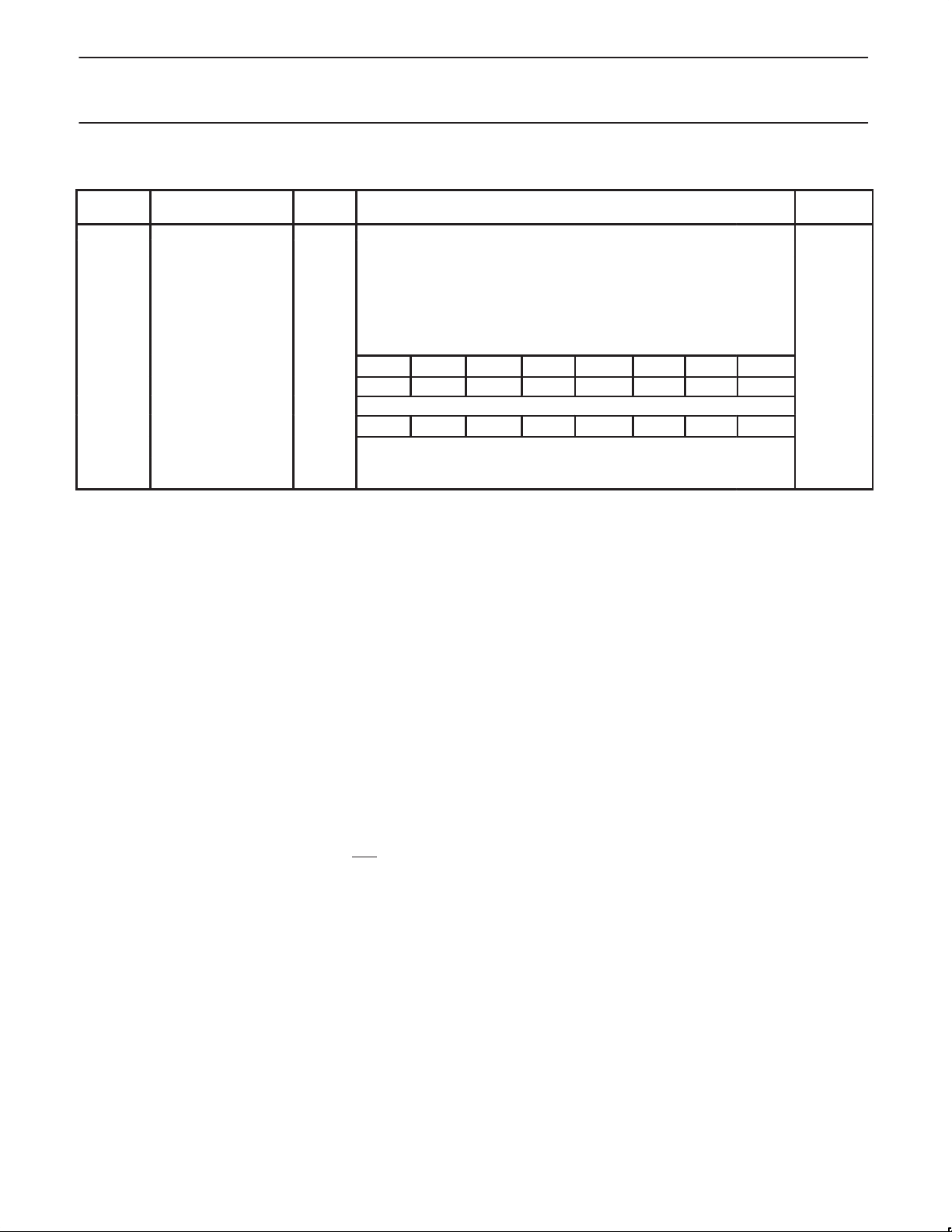
Table 1. 87C576 Special Function Registers (Continued)
SYMBOL DESCRIPTION
IP0* Interrupt Priority 0 B8H – PPC PT2 PS PT1 PX1 PT0 PX0 x0000000B
IP1*# Interrupt Priority 1 F8H POB PIB PAD PC4 PC3 PC2 PC1 PC0 00H
P0* Port 0 80H AD7 AD6 AD5 AD4 AD3 AD2 AD1 AD0 FFH
P1* Port 1 90H – – ADIN5 ADIN4 ADIN3 ADIN2 ADIN1 ADIN0 FFH
P2* Port 2 A0H ECI CEX4 T2 T2EX CEX3 CEX2 CEX1 CEX0 FFH
P3* Port 3 B0H RD WR T1 T0 INT1 INT0 TxD RxD FFH
P0M1# Port 0 Output Mode 1 84H 00H
P0M2# Port 0 Output Mode 2 85H 00H
P1M1# Port 1 Output Mode 1 94H 00H
P1M2# Port 1 Output Mode 2 95H 3FH
P2M1# Port 2 Output Mode 1 A4H 00H
P2M2# Port 2 Output Mode 2 A5H FFH
P3M1# Port 3 Output Mode 1 B4H 00H
P3M2# Port 3 Output Mode 2 B5H FFH
PCON Power Control 87H
PSW* Program Status Word D0H CY AC F0 RS1 RS0 OV – P 00H
PWCON# PWM Control BCH – – – – PWMF
PWMP# PWM Prescaler BDH 00H
PWM0# PWM Register 0 BEH 00H
PWM1# PWM Register 1 BFH 00H
RACAP2H#
RACAP2L#
Timer 2 Capture High CBH 00H
Timer 2 Capture Low CAH 00H
DIRECT
ADDRESS
BIT ADDRESS, SYMBOL, OR ALTERNATIVE PORT FUNCTION
MSB LSB
BF BE BD BC BB BA B9 B8
87 86 85 84 83 82 81 80
97 96 95 94 93 92 91 90
A7 A6 A5 A4 A3 A2 A1 A0
B7 B6 B5 B4 B3 B2 B1 B0
1
SMOD1
SMOD0
D7 D6 D5 D4 D3 D2 D1 D0
OSF1POF1LVF
WDT0F
EN/CLR
83C576/87C576
1
PD IDL 00xxxx00B
PWE1 PWE0 00H
RESET
VALUE
SADDR# Slave Address A9H 00H
SADEN# Slave Address Mask B9H 00H
SBUF Serial Data Buffer 99H xxxxxxxxB
9F 9E 9D 9C 9B 9A 99 98
SCON* Serial Control 98H
SP Stack Pointer 81H 07H
TCON* Timer Control 88H TF1 TR1 TF0 TR0 IE1 IT1 IE0 IT0 00H
T2CON* Timer 2 Control C8H TF2 EXF2 RCLK TCLK EXEN2 TR2 C/T2 CP/RL2 00H
T2MOD# Timer 2 Mode Control C9H – – – – – – T2OE2DCEN xxxxxxx0B
* SFRs are bit addressable.
# SFRs are modified from or added to the 80C51 SFRs.
1. Reset value depends on reset source.
2. Programmable clock-out
1998 Jun 04
SM0/FE
8F 8E 8D 8C 8B 8A 89 88
CF CE CD CC CB CA C9 C8
SM1 SM2 REN TB8 RB8 TI RI 00H
8
Philips Semiconductors Product specification
80C51 8-bit microcontroller family
8K/256 OTP/ROM, 6 channel 10-bit A/D, 4 comparators,
failure detect circuitry, watchdog timer
Table 1. 87C576 Special Function Registers (Continued)
SYMBOL DESCRIPTION
TH0 Timer High 0 8CH 00H
TH1 Timer High 1 8DH 00H
TH2# Timer High 2 CDH 00H
TL0 Timer Low 0 8AH 00H
TL1 Timer Low 1 8BH 00H
TL2# Timer Low 2 CCH 00H
TMOD Timer Mode 89H GATE C/T M1 M0 GATE C/T M1 M0 00H
UCS# UPI Control/Status 86H
DIRECT
ADDRESS
BIT ADDRESS, SYMBOL, OR ALTERNATIVE PORT FUNCTION
MSB LSB
ST7 ST6 ST5 ST4 UE AF IBF
83C576/87C576
RESET
VALUE
OBE/OBF
00H
WDCON#Watchdog Timer Control
WDL#
WFEED1# Watchdog Feed 1 C2H xxH
WFEED2# Watchdog Feed 2 C3H xxH
* SFRs are bit addressable.
# SFRs are modified from or added to the 80C51 SFRs.
1. Reset value depends on reset source.
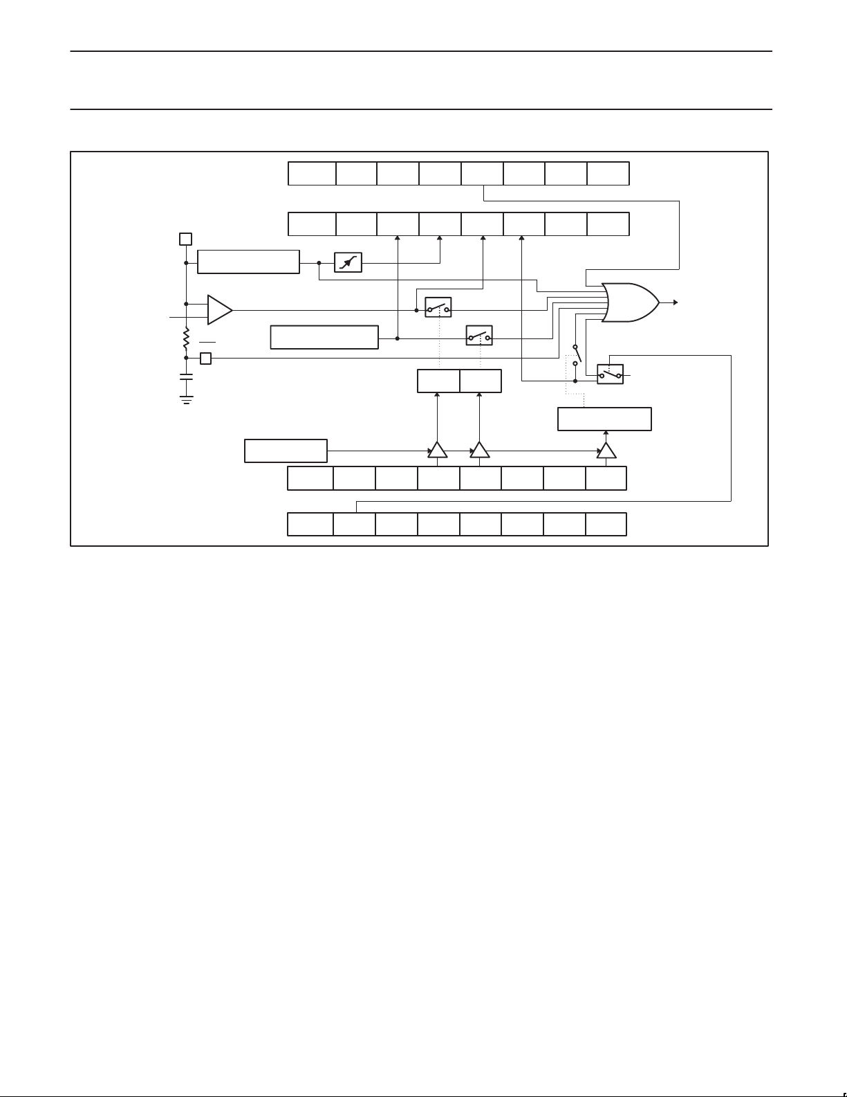
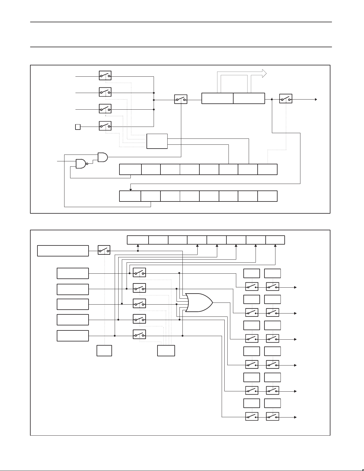
The 8XC576 has a number of failure detect circuits to prevent
abnormal operating conditions. these failure detect circuits generate
resets as shown in Figure 1.
Watchdog Timer Reload
POWER ON CLEAR / POWER ON FLAG
An on-chip Power On Detect Circuit resets the 8XC576 and sets the
Power Off Flag (PCON.4) on power up or if V
momentarily. The POF can only be cleared by software. The RST
pin is not driven by the power on detect circuit. The POF can be
read by software to determine that a power failure has occurred and
can also be set by software.
LOW VOLTAGE DETECT
An on-chip Low Voltage Detect circuit sets the Low Voltage Flag
(PCON.3) if V
Characteristics) and resets the 8XC576 if the Low Voltage Reset
Enable bit (WDCON.4) is set. If the LVRE is cleared, the reset is
disabled but LVF will still be set if V
driven by the low voltage detect circuit. The LVF can be read by
software to determine that V
cleared by software.
drops below V
CC
LOW
was low. The LVF can be set or
CC
OSCILLATOR FAIL DETECT
An on-chip Oscillator Fail Detect circuit sets the Oscillator Fail Flag
(PCON.5) if the oscillator frequency drops below OSCF for one or
more cycles (see AC Electrical Characteristics: OSCF) and resets
the 8XC576 if the Oscillator Fail Reset Enable bit (WDCON.3) is set.
If OFRE is cleared, the reset is disabled but OSF will still be set if
the oscillator fails. The RST pin is not driven by the oscillator fail
detect circuit. The OSF can be read by software to determine that
an oscillator failure has occurred. The OSF can be set or cleared by
software.
C4H PRE2 PRE1 PRE0 LVRE OFRE DPD
C1H 00H
LOW ACTIVE RESET
One of the most notable features on this part is the low active reset.
The low active reset operates exactly the same as high active reset
with the exception that the part is put into the reset mode by
applying a low level to the reset pin. For power-on reset it is also
necessary to invert the power-on reset circuit; connecting the 8.2K
resistor from the reset pin to V
drops to zero
CC
(see DC Electrical
is low. The RST pin is not
CC
reset pin to ground. Figure 1 shows the reset related circuitry.
When reset the port pins on the 8XC576 are driven high
synchronously.
The 8XC576 also has Low voltage detection circuitry that will, if
enabled, force the part to reset when V
set level. Low Voltage Reset is enabled by a normal reset. Low
Voltage Reset can be disabled by clearing LVRE (bit 4 in the
WDCON SFR) then executing a watchdog feed sequence (A5H to
WFEED1 followed immediately by 5AH to WFEED2). In addition
there is a flag (LVF) that is set if a low voltage condition is detected.
The LVF flag is set even if the Low Voltage detection circuitry is
disabled. Notice that the Low voltage detection circuitry does not
drive the RST# pin so the LVF flag is the only way that the
microcontroller can determine if it has been reset due to a low
voltage condition.
The 8XC576 has an on-chip power-on detection circuit that sets the
POF (PCON.4) flag on power up or if the V
drops to 0V . This flag can be used to determine if the part is being
started from a power-on (cold start) or if a reset has occurred due to
another condition (warm start).
The 8XC576 can be reset in software by setting the RST bit of the
AUXR register (AUXR.3). See Figure 1 for reset diagram.
WDRUN
and the 10µf capacitor from the
CC
WDMOD
(on the part) fails below a
CC
level momentarily
CC
11111111B
1998 Jun 04
9
Philips Semiconductors Product specification
80C51 8-bit microcontroller family
8K/256 OTP/ROM, 6 channel 10-bit A/D, 4 comparators,
failure detect circuitry, watchdog timer
83C576/87C576
VLOW
(LOW V
CC
REFERENCE)
– – – SRST TXI LO AO
V
CC
POWER-ON DETECT
+
–
RST
WATCHDOG FEED
SMOD1 SMOD0 OSF LVF WDTOF PD IDL
OSC FREQ BELOW OSCF
(MIN FREQUENCY)
SHADOW REGISTER
FOR WDCON
PRE2 PRE1 PRE0 LVRE OFRE DPD WDRUN WDMOD
CIDL WDTE – – – CPS1 CPS0 ECF
–
POF
SHADOW REGISTER
AUXR
(8EH)
PCON
(87H)
8xC576
INTERNAL
RESET
WDTE
PCA WATCHDOG
WATCHDOG TIMER
WDCON
(C4H)
CMOD
(D9H)
SU00515B
Figure 1. Reset Circuitry
TIMERS
The 8XC576 has four on-chip timers.
Timers 0 and 1 are identical in every way to Timers 0 and 1 on the
80C51.
Timer 2 on the 8XC576 is identical to the 80C52 Timer 2 (described
in detail in the 80C52 overview) with the exception that it is an up or
down counter. To configure the Timer to count down the DCEN bit in
the T2MOD special function register must be set and a low level
must be present on the T2EX pin (P1.1).
The Pulse Width Modulator (PWM) system can be used as a timer
by disabling its outputs and monitoring its counter overflow flag, the
PWMF bit in the PWCON register (see the PWM section for details).
The Watchdog timer operation and implementation is similar to the
8XC550 (for additional information see the 8XC550 datasheet) with
the exception that the reset values of the WDCON and WDL special
function registers have been changed. The changes in these
registers cause the watchdog timer to be enabled with a timeout of
16384 × T
when the part is reset. The watchdog can be disabled
OSC
by executing a valid feed sequence and then clearing WDRUN (bit 2
in the WDCON SFR). In timer mode, the timer is controlled by
toggling the WDRUN bit. The timeout flag, WDTOF, is set when the
timer overflows and must be cleared in software.
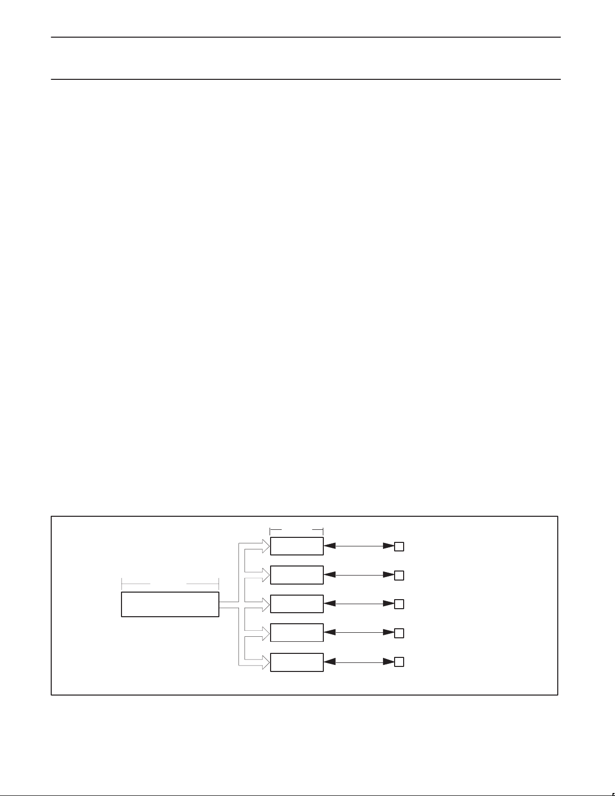
PROGRAMMABLE COUNTER ARRAY (PCA)
The Programmable Counter Array is a special Timer that has five
16-bit capture/compare modules associated with it. Each of the
modules can be programmed to operate in one of four modes: rising
and/or falling edge capture, software timer, high-speed output, or
pulse width modulator . Each module has a pin associated with it in
port 2. Module 0 is connected to P2.0(CEX0), module 1 to
P2.1(CEX1), etc. The basic PCA configuration is shown in Figure 2.
The PCA timer is a common time base for all five modules and can
be programmed to run at: 1/12 the oscillator frequency, 1/4 the
oscillator frequency , the Timer 0 overflow, or the input on the ECI pin
(P2.7). The timer count source is determined from the CPS1 and
CPS0 bits in the CMOD SFR as follows (see Figure 3):
CPS1 CPS0 PCA Timer Count Source
0 0 1/12 oscillator frequency
0 1 1/4 oscillator frequency
1 0 Timer 0 overflow
1 1 External Input at ECI pin (P2.7)
In the CMOD SFR are three additional bits associated with the PCA.
They are CIDL which allows the PCA to stop during idle mode,
WDTE which enables or disables the watchdog function on
module 4, and ECF which when set causes an interrupt and the
PCA overflow flag CF (in the CCON SFR) to be set when the PCA
timer overflows. These functions are shown in Figure 3.
The watchdog timer function is implemented in module 4 as
implemented in other parts that have a PCA that are available on the
market. However, if a watchdog timer is required in the target
application, it is recommended to use the hardware watchdog timer
that is implemented on the 87C576 separately from the PCA (see
Figure 15).
The CCON SFR contains the run control bit for the PCA and the
flags for the PCA timer (CF) and each module (refer to Figure 6). To
run the PCA the CR bit (CCON.6) must be set by software. The
PCA is shut off by clearing this bit. The CF bit (CCON.7) is set when
the PCA counter overflows and an interrupt will be generated if the
ECF bit in the CMOD register is set, The CF bit can only be cleared
by software. Bits 0 through 4 of the CCON register are the flags for
the modules (bit 0 for module 0, bit 1 for module 1, etc.) and are set
by hardware when either a match or a capture occurs. These flags
1998 Jun 04
10
Philips Semiconductors Product specification
80C51 8-bit microcontroller family
8K/256 OTP/ROM, 6 channel 10-bit A/D, 4 comparators,
failure detect circuitry, watchdog timer
83C576/87C576
also can only be cleared by software. The PCA interrupt system
shown in Figure 4.
Each module in the PCA has a special function register associated
with it. These registers are: CCAPM0 for module 0, CCAPM1 for
module 1, etc. (see Figure 7). The registers contain the bits that
control the mode that each module will operate in. The ECCF bit
(CCAPMn.0 where n=0, 1, 2, 3, or 4 depending on the module)
enables the CCF flag in the CCON SFR to generate an interrupt
when a match or compare occurs in the associated module. PWM
(CCAPMn.1) enables the pulse width modulation mode. The TOG
bit (CCAPMn.2) when set causes the CEX output associated with
the module to toggle when there is a match between the PCA
counter and the module’s capture/compare register. The match bit
MAT (CCAPMn.3) when set will cause the CCFn bit in the CCON
register to be set when there is a match between the PCA counter
and the module’s capture/compare register.
The next two bits CAPN (CCAPMn.4) and CAPP (CCAPMn.5)
determine the edge that a capture input will be active on. The CAPN
bit enables the negative edge, and the CAPP bit enables the
positive edge. If both bits are set both edges will be enabled and a
capture will occur for either transition. The last bit in the register
ECOM (CCAPMn.6) when set enables the comparator function.
Figure 8 shows the CCAPMn settings for the various PCA functions.
There are two additional registers associated with each of the PCA
modules. They are CCAPnH and CCAPnL and these are the
registers that store the 16-bit count when a capture occurs or a
compare should occur. When a module is used in the PWM mode
these registers are used to control the duty cycle of the output.
PCA Capture Mode
To use one of the PCA modules in the capture mode either one or
both of the CCAPM bits CAPN and CAPP for that module must be
set. The external CEX input for the module (on port 2) is sampled for
a transition. When a valid transition occurs the PCA hardware loads
the value of the PCA counter registers (CH and CL) into the
module’s capture registers (CCAPnL and CCAPnH). If the CCFn bit
for the module in the CCON SFR and the ECCFn bit in the CCAPMn
SFR are set then an interrupt will be generated. Refer to Figure 9.
16-bit Software Timer Mode
The PCA modules can be used as software timers by setting both
the ECOM and MAT bits in the modules CCAPMn register. The PCA
timer will be compared to the module’s capture registers and when a
match occurs an interrupt will occur if the CCFn (CCON SFR) and
the ECCFn (CCAPMn SFR) bits for the module are both set (see
Figure 10).
High Speed Output Mode
In this mode the CEX output (on port 2) associated with the PCA
module will toggle each time a match occurs between the PCA
counter and the module’s capture registers. To activate this mode
the TOG, MAT, and ECOM bits in the module’s CCAPMn SFR must
be set (see Figure 11).
Pulse Width Modulator Mode
All of the PCA modules can be used as PWM outputs. Figure 12
shows the PWM function. The frequency of the output depends on
the source for the PCA timer. All of the modules will have the same
frequency of output because they all share the PCA timer. The duty
cycle of each module is independently variable using the module’s
capture register CCAPLn. When the value of the PCA CL SFR is
less than the value in the module’s CCAPLn SFR the output will be
low, when it is equal to or greater than the output will be high. When
CL overflows from FF to 00, CCAPLn is reloaded with the value in
CCAPHn. the allows updating the PWM without glitches. The PWM
and ECOM bits in the module’s CCAPMn register must be set to
enable the PWM mode.
PCA Interrupt System
The PCA on most 80C51 family devices provides a single interrupt
source, EC (IE.6). The 8xC576 expands the flexibility of the PCA by
providing additional interrupt sources for each of the five PCA
modules, EC0 (IE1.0) through EC4 (IE1.4), in addition to the original
interrupt source EC (IE.6). Any of these sources can be enabled at
any time. It is possible for both a module source (EC0 through EC4)
to be enabled at the same time that the single source, EC, is
enabled. In this case, a module event will generate an interrupt for
both the module source and the single source, EC.
MODULE FUNCTIONS:
16-BIT CAPTURE
16-BIT TIMER
16-BIT HIGH SPEED OUTPUT
8-BIT PWM
WATCHDOG TIMER (MODULE 4 ONLY)
1998 Jun 04
16 BITS
PCA TIMER/COUNTER
TIME BASE FOR PCA MODULES
16 BITS
MODULE 0
MODULE 1
MODULE 2
MODULE 3
MODULE 4
Figure 2. Programmable Counter Array (PCA)
11
P2.0/CEX0
P2.1/CEX1
P2.2/CEX2
P2.3/CEX3
P2.6/CEX4
SU00578
Philips Semiconductors Product specification
80C51 8-bit microcontroller family
8K/256 OTP/ROM, 6 channel 10-bit A/D, 4 comparators,
failure detect circuitry, watchdog timer
OSC/12
83C576/87C576
TO PCA
MODULES
OSC/4
TIMER 0
OVERFLOW
EXTERNAL INPUT
(P2.7/ECI)
IDLE
PCA TIMER/COUNTER
OVERFLOW
CH CL
16–BIT UP COUNTER
00
01
10
DECODE
11
CIDL WDTE –– –– –– CPS1 CPS0 ECF
CF CR CCF4 CCF3 CCF2 CCF1 CCF0––
Figure 3. PCA Timer/Counter
CF CR CCF4 CCF3 CCF2 CCF1 CCF0––
CMOD
(D9H)
CCON
(D8H)
CCON
(D8H)
INTERRUPT
SU00516
MODULE 0
MODULE 1
MODULE 2
MODULE 3
MODULE 4
CMOD.0 ECF
CCAPMn.0 ECCFn
Figure 4. PCA Interrupt System
IE1.0
EC0
IE1.1
EC1
IE0.6
EC
IE1.2
EC2
IE1.3
EC3
IE1.4
EC4
IE0.7
EA
IE0.7
EA
IE0.7
EA
IE0.7
EA
IE0.7
EA
IE0.7
EA
TO
INTERRUPT
PRIORITY
DECODER
TO
INTERRUPT
PRIORITY
DECODER
TO
INTERRUPT
PRIORITY
DECODER
TO
INTERRUPT
PRIORITY
DECODER
TO
INTERRUPT
PRIORITY
DECODER
TO
INTERRUPT
PRIORITY
DECODER
SU00579
1998 Jun 04
12

Philips Semiconductors Product specification
80C51 8-bit microcontroller family
8K/256 OTP/ROM, 6 channel 10-bit A/D, 4 comparators,
failure detect circuitry, watchdog timer
83C576/87C576
CMOD Address = OD9H
Reset Value = 00XX X000B
CIDL WDTE – – – CPS1 CPS0 ECF
Bit:
76543210
Symbol Function
CIDL Counter Idle control: CIDL = 0 programs the PCA Counter to continue functioning during idle Mode.
CIDL = 1 programs it to be gated off during idle.
WDTE Watchdog Timer Enable: WDTE = 0 disables Watchdog Timer function on PCA Module 4. WDTE = 1 enables it.
– Not implemented, reserved for future use.*
CPS1 PCA Count Pulse Select bit 1.
CPS0 PCA Count Pulse Select bit 0.
CPS1 CPS0 Selected PCA Input**
0 0 0 Internal clock, f
0 1 1 Internal clock, f
OSC
OSC
÷ 12
÷ 4
1 0 2 Timer 0 overflow
1 1 3 External clock at ECI/P2.7 pin (max. rate = f
OSC
÷ 8)
ECF PCA Enable Counter Overflow interrupt:
ECF = 1 enables CF bit in CCON to generate an interrupt. ECF = 0 disables that function of CF.
NOTE:
* User software should not write 1s to reserved bits. These bits may be used in future 8051 family products to invoke new features. In that case, the reset or inactive value of the
new bit will be 0, and its active value will be 1. The value read from a reserved bit is indeterminate.
= oscillator frequency
** –f
OSC
SU00686A
Figure 5. CMOD: PCA Counter Mode Register
CCON Address = OD8H
Reset Value = 00X0 0000B
Bit Addressable
CF CR – CCF4 CCF3 CCF2 CCF1 CCF0
Bit:
76543210
Symbol Function
CF PCA Counter Overflow flag. Set by hardware when the counter rolls over. CF flags an interrupt if bit ECF in CMOD is
set. CF may be set by either hardware or software but can only be cleared by software.
CR PCA Counter Run control bit. Set by software to turn the PCA counter on. Must be cleared by software to turn the PCA
counter off.
– Not implemented, reserved for future use*.
CCF4 PCA Module 4 interrupt flag. Set by hardware when a match or capture occurs. Must be cleared by software.
CCF3 PCA Module 3 interrupt flag. Set by hardware when a match or capture occurs. Must be cleared by software.
CCF2 PCA Module 2 interrupt flag. Set by hardware when a match or capture occurs. Must be cleared by software.
CCF1 PCA Module 1 interrupt flag. Set by hardware when a match or capture occurs. Must be cleared by software.
CCF0 PCA Module 0 interrupt flag. Set by hardware when a match or capture occurs. Must be cleared by software.
NOTE:
* User software should not write 1s to reserved bits. These bits may be used in future 8051 family products to invoke new features. In that case, the reset or inactive value of the
new bit will be 0, and its active value will be 1. The value read from a reserved bit is indeterminate.
SU00036
Figure 6. CCON: PCA Counter Control Register
1998 Jun 04
13

Philips Semiconductors Product specification
80C51 8-bit microcontroller family
8K/256 OTP/ROM, 6 channel 10-bit A/D, 4 comparators,
failure detect circuitry, watchdog timer
83C576/87C576
CCAPMn Address CCAPM0 0DAH
Not Bit Addressable
Bit:
Symbol Function
– Not implemented, reserved for future use*.
ECOMn Enable Comparator. ECOMn = 1 enables the comparator function.
CAPPn Capture Positive, CAPPn = 1 enables positive edge capture.
CAPNn Capture Negative, CAPNn = 1 enables negative edge capture.
MATn Match. When MATn = 1, a match of the PCA counter with this module’s compare/capture register causes the CCFn bit
TOGn Toggle. When TOGn = 1, a match of the PCA counter with this module’s compare/capture register causes the CEXn
PWMn Pulse Width Modulation Mode. PWMn = 1 enables the CEXn pin to be used as a pulse width modulated output.
ECCFn Enable CCF interrupt. Enables compare/capture flag CCFn in the CCON register to generate an interrupt.
NOTE:
*User software should not write 1s to reserved bits. These bits may be used in future 8051 family products to invoke new features. In that case, the reset or inactive value of the new
bit will be 0, and its active value will be 1. The value read from a reserved bit is indeterminate.
in CCON to be set, flagging an interrupt.
pin to toggle.
CCAPM1 0DBH
CCAPM2 0DCH
CCAPM3 0DDH
CCAPM4 0DEH
– ECOMn CAPPn CAPNn MATn TOGn PWMn ECCFn
76543210
Figure 7. CCAPMn: PCA Modules Compare/Capture Registers
Reset Value = X000 0000B
SU00037
ECOMn CAPPn CAPNn MATn TOGn PWMn ECCFn MODULE FUNCTION
–
X 0 0 0 0 0 0 0 No operation
X X 1 0 0 0 0 X 16-bit capture by a positive-edge trigger on CEXn
X X 0 1 0 0 0 X 16-bit capture by a negative trigger on CEXn
X X 1 1 0 0 0 X 16-bit capture by a transition on CEXn
X 1 0 0 1 0 0 X 16-bit Software Timer
X 1 0 0 1 1 0 X 16-bit High Speed Output
X 1 0 0 0 0 1 0 8-bit PWM
X 1 0 0 1 X 0 X Watchdog Timer
Figure 8. PCA Module Modes (CCAPMn Register)
1998 Jun 04
14
 Loading...