

Philips 74LVU04N, 74LVU04DB, 74LVU04D, 74LVU04PW Datasheet
INTEGRATED CIRCUITS
74LVU04
Hex inverter
Product specification
Supersedes data of 1997 Feb 12
IC24 Data Handbook
1998 Apr 20
Philips Semiconductors Product specification
74L VU04Hex inverter
FEA TURES
•Wide operating voltage: 1.0 to 5.5 V
•Optimized for Low Voltage applications: 1.0 to 3.6 V
•Accepts TTL input levels between V
•Typical V
T
amb
•Typical V
T
amb
(output ground bounce) < 0.8 V at VCC = 3.3 V,
OLP
= 25°C.
(output VOH undershoot) > 2 V at VCC = 3.3 V,
OHV
= 25°C.
= 2.7 V and VCC = 3.6 V
CC
•Output capability: standard
•I
category: SSI
CC
QUICK REFERENCE DATA
GND = 0 V; T
SYMBOL
t
NOTES:
1. C
is used to determine the dynamic power dissipation (PD in µW)
PD
= CPD V
P
D
f
= input frequency in MHz; CL = output load capacitance in pF;
i
= output frequency in MHz; VCC = supply voltage in V;
f
o
(C
L
2. The condition is V
= 25°C; tr = tf 2.5 ns
amb
PHL/tPLH
C
I
C
PD
CC
2
V
fo) = sum of the outputs.
CC
PARAMETER CONDITIONS TYPICAL UNIT
Propagation delay
nA to nY
Input capacitance 3.5 pF
Power dissipation capacitance per gate Notes 1, 2 18 pF
2
fi (CL V
= GND to V
I
CC.
2
fo) where:
CC
DESCRIPTION
The 74LVU04 is a low-voltage, Si-gate CMOS device and is pin
compatible with the 74HCU04.
The 74LVU04 is a general purpose hex inverter. Each of the six
inverters is a single stage with unbuffered outputs.
CL = 15 pF;
VCC = 3.3 V
6 ns
ORDERING INFORMATION
PACKAGES TEMPERATURE RANGE OUTSIDE NORTH AMERICA NORTH AMERICA PKG. DWG. #
14-Pin Plastic DIL –40°C to +125°C 74LVU04 N 74LVU04 N SOT27-1
14-Pin Plastic SO –40°C to +125°C 74LVU04 D 74LVU04 D SOT108-1
14-Pin Plastic SSOP Type II –40°C to +125°C 74LVU04 DB 74LVU04 DB SOT337-1
14-Pin Plastic TSSOP Type I –40°C to +125°C 74LVU04 PW 74LVU04PW DH SOT402-1
PIN DESCRIPTION
PIN NUMBER SYMBOL NAME AND FUNCTION
1, 3, 5, 9, 11, 13 1A – 6A Data inputs
2, 4, 6, 8, 10, 12 1Y – 6Y Data outputs
7 GND Ground (0 V)
14 V
CC
Positive supply voltage
FUNCTION TABLE
INPUTS OUTPUTS
nA nY
L H
H L
NOTES:
H = HIGH voltage level
L = LOW voltage level
1998 Apr 20 853–1918 19257
2

Philips Semiconductors Product specification
Hex inverter
PIN CONFIGURATION
1
1A
2
1Y
3
2A
4
2Y
5
3A
6
3Y
GND
7
LOGIC SYMBOL (IEEE/IEC)
12
34
56
1
1
1
14
V
13
6A
12
6Y
11
5A
10
5Y
9
4A
8
4Y
SV00396
CC
74LVU04
LOGIC SYMBOL
2Y
6Y
SV00397
V
CCVCC
2
4
6
8
10
12
1A 1Y
1
2A
3
5
3A 3Y
4A 4Y
9
11
5A 5Y
6A
13
SCHEMATIC DIAGRAM (ONE INVERTER)
V
CC
98
11 10
13 12
1
1
1
SV00398
100
nA nY
170
SV00400
RECOMMENDED OPERATING CONDITIONS
SYMBOL PARAMETER CONDITIONS MIN TYP. MAX UNIT
V
V
V
T
amb
tr, t
NOTE:
1. The LV is guaranteed to function down to V
DC supply voltage See Note1 1.0 3.3 5.5 V
CC
Input voltage 0 – V
I
Output voltage 0 – V
O
Operating ambient temperature range in free air
Input rise and fall times
f
CC
See DC and AC
characteristics
VCC = 1.0V to 2.0V
VCC = 2.0V to 2.7V
VCC = 2.7V to 3.6V
VCC = 3.6V to 5.5V
= 1.0V (input levels GND or VCC); DC characteristics are guaranteed from VCC = 1.2V to VCC = 5.5V.
–40
–40
–
–
–
–
–
–
–
–
CC
CC
+85
+125
500
200
100
50
ns/V
V
V
°C
1998 Apr 20
3
Philips Semiconductors Product specification
V
V
V
V
voltage
V
V
voltage
Hex inverter
ABSOLUTE MAXIMUM RATINGS
1, 2
74LVU04
In accordance with the Absolute Maximum Rating System (IEC 134).
Voltages are referenced to GND (ground = 0V).
SYMBOL
V
CC
I
IK
I
OK
I
O
I
GND
I
CC
T
stg
P
TOT
DC supply voltage –0.5 to +7.0 V
DC input diode current VI < –0.5 or VI > VCC + 0.5V 20 mA
DC output diode current VO < –0.5 or VO > VCC + 0.5V 50 mA
DC output source or sink current
– standard outputs
DC VCC or GND current for types with
,
– standard outputs 50
Storage temperature range –65 to +150 °C
Power dissipation per package
– plastic DIL
– plastic mini-pack (SO)
– plastic shrink mini-pack (SSOP and TSSOP)
PARAMETER CONDITIONS RATING UNIT
–0.5V < VO < VCC + 0.5V
25
mA
mA
for temperature range: –40 to +125°C
above +70°C derate linearly with 12 mW/K
above +70°C derate linearly with 8 mW/K
above +60°C derate linearly with 5.5 mW/K
750
500
400
mW
NOTE:
1. Stresses beyond those listed may cause permanent damage to the device. These are stress ratings only and functional operation of the
device at these or any other conditions beyond those indicated under “recommended operating conditions” is not implied. Exposure to
absolute-maximum-rated conditions for extended periods may affect device reliability .
2. The input and output voltage ratings may be exceeded if the input and output current ratings are observed.
DC ELECTRICAL CHARACTERISTICS
Over recommended operating conditions. V oltages are referenced to GND (ground = 0V).
SYMBOL P ARAMETER TEST CONDITIONS
VCC = 1.2V 1.0 1.0
IH
HIGH level Input
voltage
VCC = 2.0V 1.6 1.6
VCC = 2.7 to 3.6V 2.4 2.4
VCC = 4.5 to 5.5V 0.8V
VCC = 1.2V 0.2 0.2
IL
LOW level Input
voltage
VCC = 2.0V 0.4 0.4
VCC = 2.7 to 3.6V 0.5 0.5
VCC = 4.5 to 5.5 0.2V
VCC = 1.2V; VI = VIH or V
VCC = 2.0V; VI = VIH or V
OH
HIGH level output
VCC = 2.7V; VI = VIH or V
V
VCC = 3.0V; VI = VIH or V
VCC = 4.5V;VI = VIH or V
OH
HIGH level output
voltage
VCC = 3.0V;VI = VIH or V
VCC = 4.5V;VI = VIH or V
VCC = 1.2V; VI = VIH or V
VCC = 2.0V; VI = VIH or V
OL
LOW level output
VCC = 2.7V; VI = VIH or V
V
VCC = 3.0V;VI = VIH or V
VCC = 4.5V;VI = VIH or V
–IO = 100µA 1.2
IL;
–IO = 100µA 1.8 2.0 1.8
IL;
–IO = 100µA 2.5 2.7 2.5
IL;
–IO = 100µA 2.8 3.0 2.8
IL;
–IO = 100µA 4.3 4.5 4.3
IL;
–IO = 6mA 2.40 2.82 2.20
IL;
–IO = 12mA 3.60 4.20 3.50
IL;
IO = 100µA 0
IL;
IO = 100µA 0 0.2 0.2
IL;
IO = 100µA 0 0.2 0.2
IL;
IO = 100µA 0 0.2 0.2
IL;
IO = 100µA 0 0.2 0.2
IL;
-40°C to +85°C -40°C to +125°C
MIN TYP
CC
LIMITS
1
MAX MIN MAX
0.8V
CC
CC
0.2V
UNIT
CC
V
V
1998 Apr 20
4
Philips Semiconductors Product specification
V
V
CONDITION
nA to nY
Hex inverter
DC ELECTRICAL CHARACTERISTICS (Continued)
SYMBOL PARAMETER TEST CONDITIONS
LOW level output
OL
voltage
±I
I
∆I
Input leakage current VCC = 5.5V; VI = VCC or GND 1.0 1.0 µA
I
Quiescent supply
CC
current
Additional quiescent
CC
supply current per input
VCC = 3.0V;VI = VIH or V
VCC = 4.5V;VI = VIH or V
VCC = 5.5V; VI = VCC or GND; IO = 0 20.0 40.0 µA
VCC = 2.7V to 3.6V; VI = VCC –0.6V 500 850 µA
NOTE:
1. All typical values are measured at T
amb
= 25°C.
AC CHARACTERISTICS
GND = 0V; tr = tf = 2.5ns; CL = 50pF; RL = 500Ω
SYMBOL PARAMETER WAVEFORM
t
PHL/PLH
NOTES:
1. Unless otherwise stated, all typical values are measured at T
2. Typical values are measured at V
Propagation delay
= 3.3 V.
CC
Figure 1
IL;
IL;
3.0 to 3.6 7
4.5 to 5.5 7 9
amb
74LVU04
LIMITS
-40°C to +85°C -40°C to +125°C
MIN TYP
IO = 6mA 0.25 0.40 0.50
IO = 12mA 0.35 0.55 0.65
VCC(V) MIN TYP
1.2 35
2.0 12 14 17
2.7 9 10 13
= 25°C
1
MAX MIN MAX
LIMITS
–40 to +85 °C –40 to +125 °C
1
MAX MIN MAX
2
8 10
UNIT
UNIT
ns
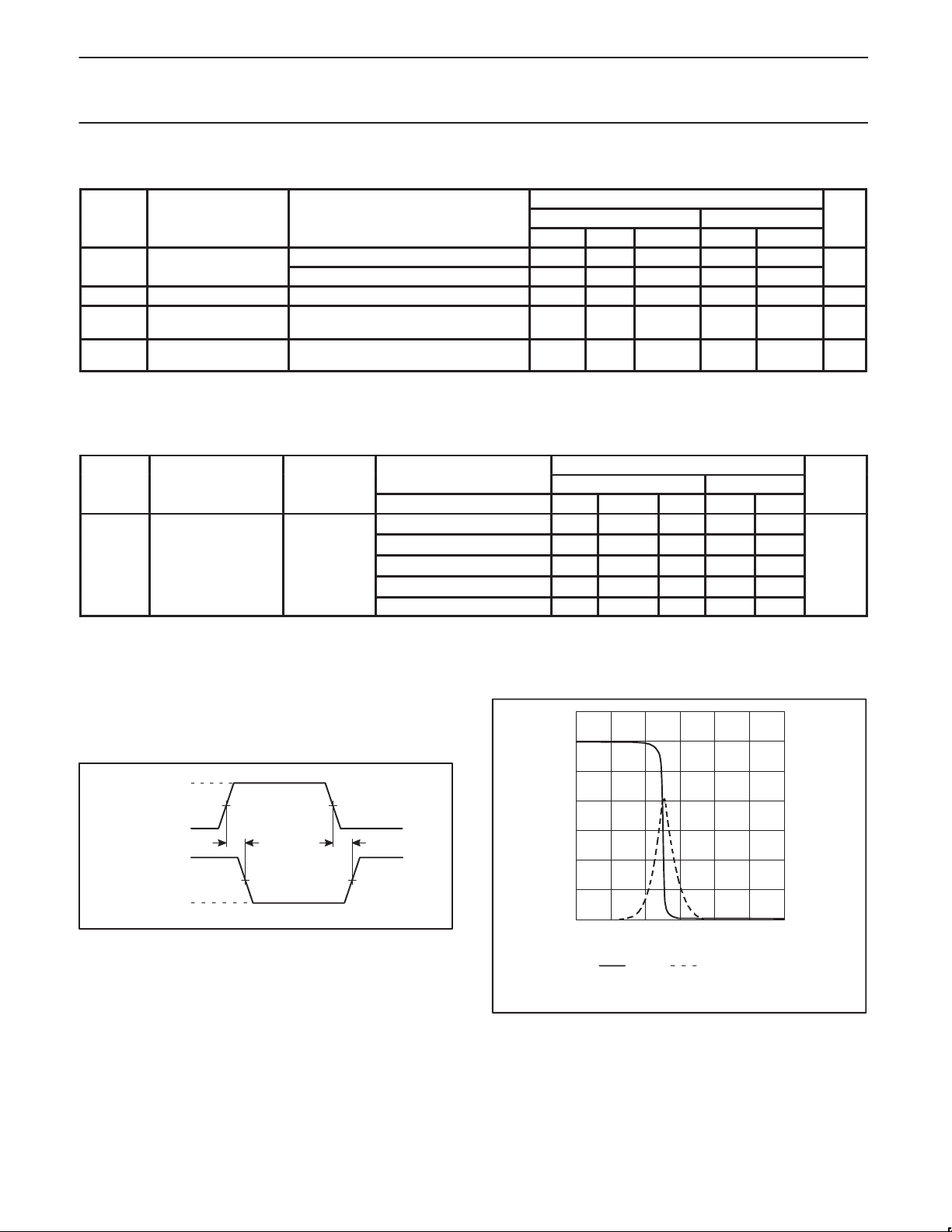
AC WAVEFORMS
VM = 1.5 V at VCC 2.7 V and ≤ 3.6 V
V
= 0.5 × VCC at VCC < 2.7 V and ≥ 4.5 V
M
V
and VOH are the typical output voltage drop that occur with the
OL
output load.
V
I
nA INPUT
GND
V
OH
nY OUTPUT
V
OL
Figure 1. Input (nA) to output (nY) propagation delays
and output transition times.
V
M
t
PHL
V
M
t
PLH
SV00395
TYPICAL TRANSFER CHARACTERISTICS
1.2
V
o
(V)
0.8
0.4
0
0 0.4 0.8
V
O
VCC = 1.2 V; IO = 0 V.
I
Figure 2.
Vi (V)
D
1.2
SV00401
300
200
100
0
I
D
(mA)
1998 Apr 20
5
 Loading...