

Philips 74LVT623PW, 74LVT623DB, 74LVT623D Datasheet

INTEGRATED CIRCUITS
74LVT623
3.3 V octal transceiver with dual enable
(3-State)
Product specification
Supersedes data of 1996 Feb 15
IC24 Data Handbook
1999 Jul 09
Philips Semiconductors Product specification
74L VT6233.3 V octal transceiver with dual enable (3-State)
FEA TURES
•Separate controls for data flow in each direction
•Output capability: +64 mA/–32 mA
•TTL input and output switching levels
•Input and output interface capability to systems at 5 V supply
•Bus-hold data inputs eliminate the need for external pull-up
resistors to hold unused inputs
•Live insertion/extraction permitted
•No bus current loading when output is tied to 5 V bus
•Power-up 3-State
•Power-up reset
•Latch-up protection exceeds 500 mA per JEDEC Std 17
•ESD protection exceeds 2000 V per MIL STD 883 Method 3015
and 200 V per Machine Model
QUICK REFERENCE DATA
SYMBOL PARAMETER
t
PLH
t
PHL
C
C
I
CCZ
IN
I/O
Propagation delay
An to Bn or Bn to An
Input capacitance VI = 0 V or 3.0 V 4 pF
I/O capacitance Outputs disabled; V
Total supply current Outputs disabled; VCC = 3.6 V 0.13 mA
DESCRIPTION
The 74LVT623 is a high-performance BiCMOS product designed for
V
The 74LVT623 device is an octal transceiver featuring non–inverting
3-State bus compatible outputs in both send and receive directions.
The 74LVT623 is designed for asynchronous two-way
communication between data buses. The control function
implementation allows for maximum flexibility in timing. This device
allows data transmission from the A bus to the B bus or from the B
bus to the A bus, depending upon the logic levels at the Enable
inputs (OEBA
the device so that the buses are effectively isolated.
Control of data flow from B to A is similar, but using the EBA
and OEBA
T
CL = 50pF;
VCC = 3.3 V
operation at 3.3 V .
CC
and OEAB). The Enable inputs can be used to disable
inputs.
CONDITIONS
= 25°C; GND = 0V
amb
= 0 V or 3.0 V 7 pF
I/O
, LEBA,
TYPICAL UNIT
2.3
2.5
ns
ORDERING INFORMATION
PACKAGES TEMPERATURE RANGE OUTSIDE NORTH AMERICA NORTH AMERICA DWG NUMBER
24-Pin Plastic SOL –40°C to +85°C 74LVT623 D 74LVT623 D SOT137-1
24-Pin Plastic SSOP Type II –40°C to +85°C 74LVT623 DB 74LVT623 DB SOT340-1
24-Pin Plastic TSSOP Type I –40°C to +85°C 74LVT623 PW 74LVT623PW DH SOT355-1
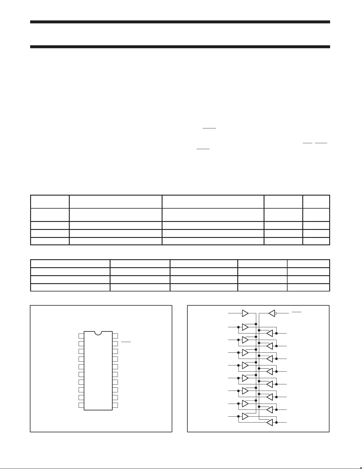
PIN CONFIGURATION
1
OEAB
2
A0
3
A1
4
A2
5
A3
6
A4
7
A5
8
A6
9
A7
10 11
GND
V
20
CC
19
OEBA
18
B0
17
B1
16
B2
15
B3
14
B4
13
B5
12
B6
B7
SA00189
LOGIC SYMBOL
OEAB
A0
A1
A2
A3
A4
A5
A6
A7
1
2
3
4
5
6
7
8
9
19
18
B0
17
B1
16
B1
15
B3
14
B4
13
B5
12
B6
11
B7
SA00195
OEBA
1999 Jul 09 853–2164 21957
2
Philips Semiconductors Product specification
I
DC output current
mA
74LVT6233.3 V octal transceiver with dual enable (3-State)
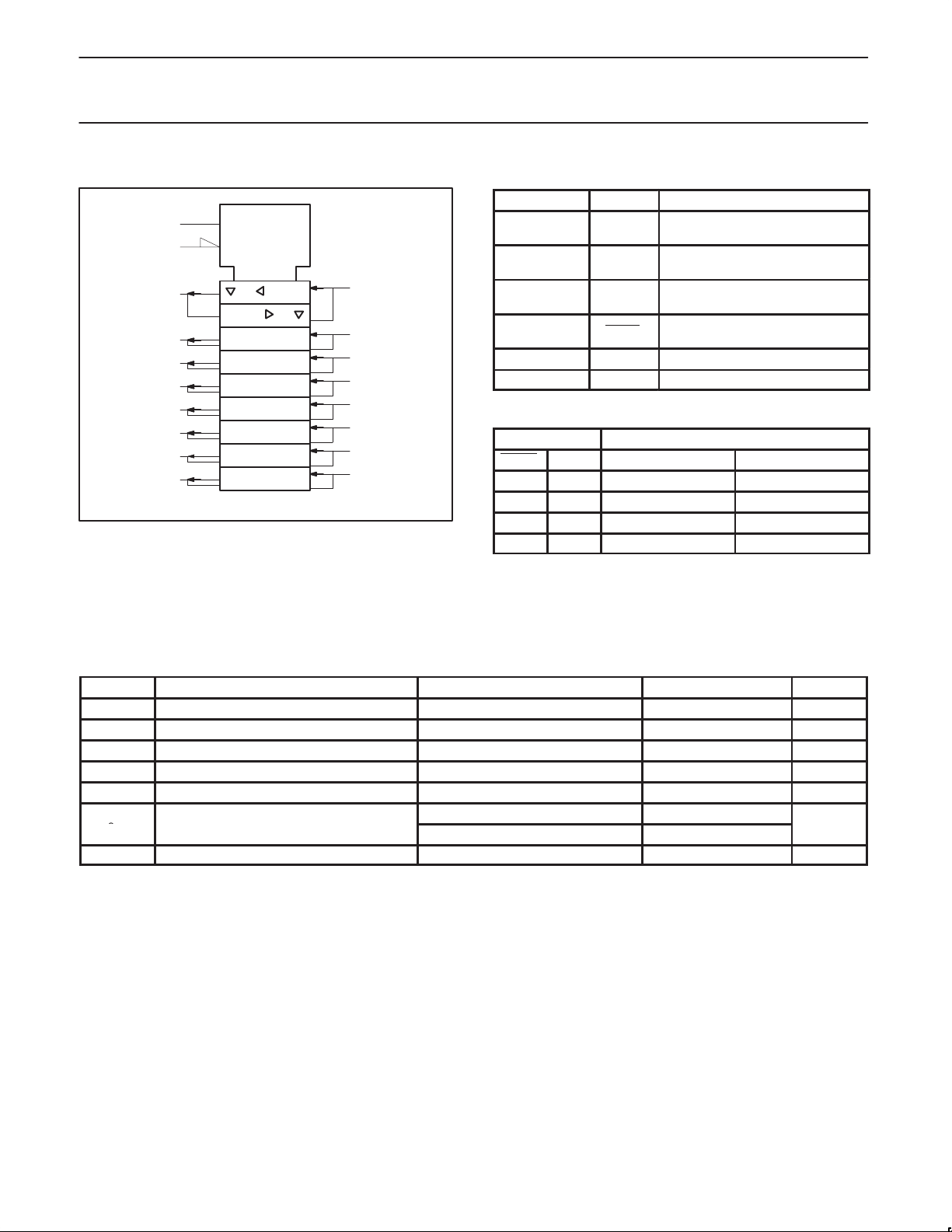
LOGIC SYMBOL (IEEE/IEC)
1
19
2
3
4
5
6
7
8
9
EN1
EN1
1
PIN DESCRIPTION
PIN NUMBER SYMBOL NAME AND FUNCTION
1 OEAB
2, 3, 4, 5,
6, 7, 8, 9
18
2
17
16
15
14
13
12
11
SA00196
18, 17, 16, 15,
14, 13, 12, 11
19 OEBA
10 GND Ground (0 V)
20 V
FUNCTION TABLE
INPUTS INPUTS/OUTPUTS
OEBA OEAB An Bn
L L An = Bn Inputs
H H Inputs Bn = An
A0 – A7 Data inputs/outputs (A side)
B0 – B7 Data inputs/outputs (B side)
H L Z Z
L H An = Bn Bn = An
H =High voltage level
L =Low voltage level
Z =High impedance “off” state
Output enable input, A side to B
side (active-High)
Output enable input, B side to A
side (active-Low)
Positive supply voltage
CC
ABSOLUTE MAXIMUM RATINGS
1, 2
SYMBOL PARAMETER CONDITIONS RATING UNIT
V
V
I
V
I
OK
OUT
OUT
T
CC
IK
stg
DC supply voltage –0.5 to +4.6 V
DC input diode current VI < 0 –50 mA
I
DC input voltage
3
–0.5 to +7.0 V
DC output diode current VO < 0 –50 mA
DC output voltage
p
3
Output in Off or High state –0.5 to +7.0 V
Output in Low state 128
Output in High state –64
Storage temperature range –65 to 150 °C
NOTES:
1. Stresses beyond those listed may cause permanent damage to the device. These are stress ratings only and functional operation of the
device at these or any other conditions beyond those indicated under “recommended operating conditions” is not implied. Exposure to
absolute-maximum-rated conditions for extended periods may affect device reliability .
2. The performance capability of a high-performance integrated circuit in conjunction with its thermal environment can create junction
temperatures which are detrimental to reliability. The maximum junction temperature of this integrated circuit should not exceed 150°C.
3. The input and output negative voltage ratings may be exceeded if the input and output clamp current ratings are observed.
1999 Jul 09
3
 Loading...