

Philips 74LVT373 Datasheet
Philips Semiconductors Low Voltage Products Objective specification
74LVT3733.3 Volt ABT octal transparent latch (3–State)
2
July 1993
FEATURES
•Designed for use in the 3.3V
high–performance market
•Supports mixed–mode signal operation; 5V
input and output voltages with 3.3V V
CC
•Bus–hold inputs eliminate the need for
external pull-up resistors to hold unused
pins
•Live insertion/extraction permitted
•No bus current loading when output is tied
to 5V bus
•8–bit transparent latch
•3-State output buffers
•Zero-static power dissipation
•Pin and function compatibility with ABT
•AC and DC performance compatibility with
ABT
•Latch–up protection exceeds 500mA per
JEDEC JC40.2 Std 17
•ESD protection exceeds 2000 V per MIL
STD 883 Method 3015 and 200 V per
Machine Model
DESCRIPTION
The 74LVT373 device is designed specifically
for low–voltage (3.3V) V
CC
operation, but can
provide a TTL interface to a 5V system
environment.
The 74LVT373 high-performance BiCMOS
device combines zero static and low dynamic
power dissipation with high speed and high
output drive.
The 74LVT373 device is an octal transparent
latch coupled to eight 3-State output buffers.
The two sections of the device are controlled
independently by Enable (E) and Output
Enable (OE
) control gates.
The data on the D inputs are transferred to
the latch outputs when the Latch Enable (E)
input is High. The latch remains transparent
to the data inputs while E is High, and stores
the data that is present one setup time before
the High-to-Low enable transition.
The 3-State output buffers are designed to
drive heavily loaded 3-State buses, MOS
memories, or MOS microprocessors. The
active-Low Output Enable (OE
) controls all
eight 3-State buffers independent of the latch
operation.
When OE
is Low, the latched or transparent
data appears at the outputs. When OE
is
High, the outputs are in the High-impedance
”OFF” state, which means they will neither
drive nor load the bus.
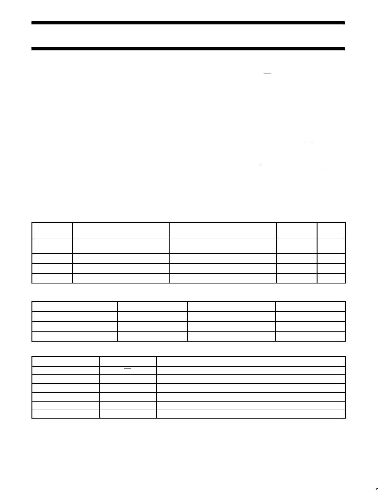
QUICK REFERENCE DATA
SYMBOL PARAMETER
CONDITIONS
T
amb
= 25°C; GND = 0V
TYPICAL UNIT
t
PLH
t
PHL
Propagation delay
Dn to Qn
CL = 50pF; VCC = 5V 4.2 ns
C
IN
Input capacitance VI = 0V or V
CC
4 pF
C
OUT
Output capacitance VI = 0V or V
CC
7 pF
I
CCZ
Total supply current Outputs disabled; VCC =5.5V 50 µA
ORDERING INFORMATION
PACKAGES TEMPERATURE RANGE ORDER CODE DRAWING NUMBER
20–Pin Plastic SOL -40°C to +85°C 74LVT373D 0172D
20–Pin Plastic SSOP -40°C to +85°C 74LVT373DB 1640B
20–Pin Plastic TSSOP -40°C to +85°C 74LVT373PW TBD
PIN DESCRIPTION
PIN NUMBER SYMBOL FUNCTION
1 OE Output enable input (active-Low)
3, 4, 7, 8, 13, 14, 17, 18 D0-D7 Data inputs
2, 5, 6, 9, 12, 15, 16, 19 Q0-Q7 Data outputs
11 E Enable input (active-High)
10 GND Ground (0V)
20 V
CC
Positive supply voltage
Philips Semiconductors Low Voltage Products Objective specification
74LVT3733.3 Volt ABT octal transparent latch (3–State)
July 1993
3
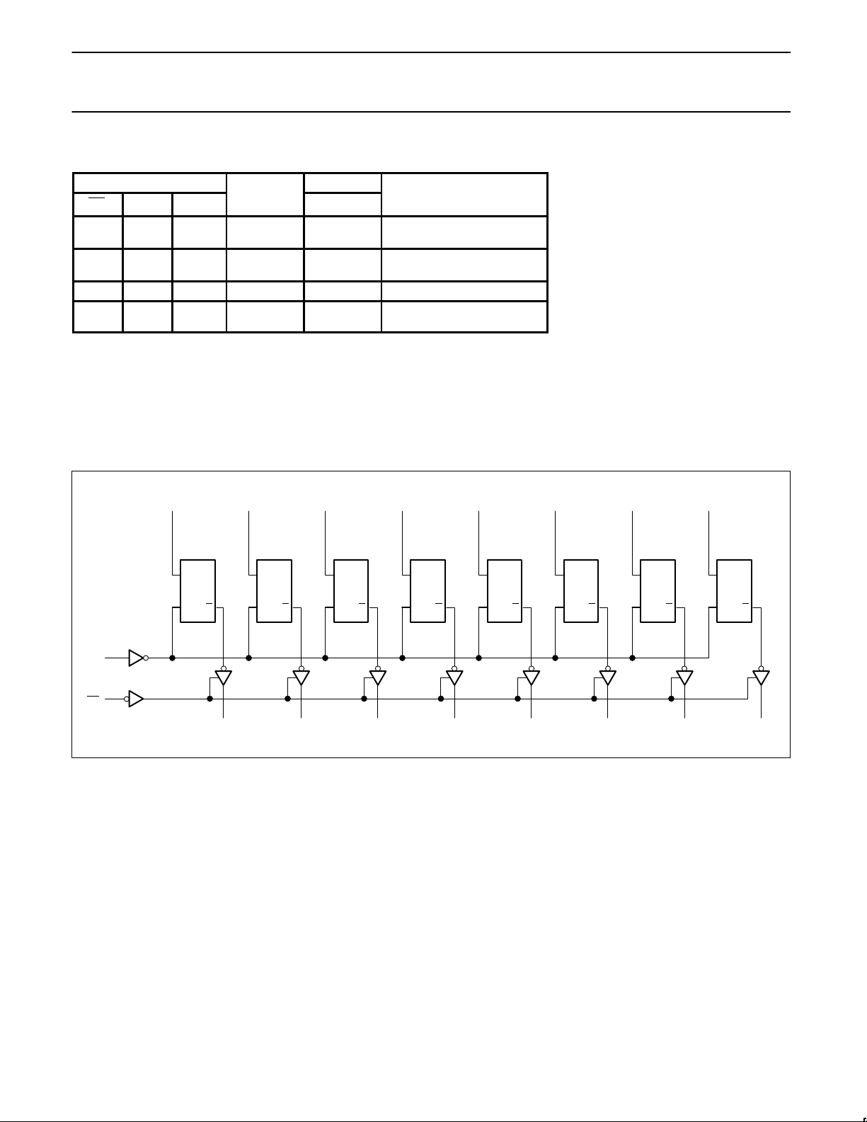
FUNCTION TABLE
INPUTS INTERNAL OUTPUTS OPERATING MODE
OE E Dn
REGISTER Q0 – Q7
L
L
H
H
L
H
L
H
L
H
Enable and read register
L
L
↓
↓
i
h
L
H
L
H
Latch and read register
L L X NC NC Hold
H
H
L
H
X
Dn
NC
Dn
Z
Z
Disable outputs
H = High voltage level
h = High voltage level one set-up time prior to the High-to-Low E transition
L = Low voltage level
l = Low voltage level one set-up time prior to the High-to-Low E transition
NC= No change
X = Don’t care
Z = High impedance “off” state
↓ = High-to-Low E transition
LOGIC DIAGRAM
E Q
D
3
D0
Q0
E Q
D
4
D1
E Q
D
7
D2
E Q
D
8
D3
E Q
D
13
D4
E Q
D
14
D5
E Q
D
17
D6
E Q
D
18
D7
2
Q1
5
Q2
6
Q3
9
Q4
12
Q5
15
Q6
16
Q7
19
11
E
1
OE
 Loading...