

Philips 74lvt32 DATASHEETS
74LVT32
3.3V Quad 2-input OR gate
Product specification 1996 Aug 28
INTEGRATED CIRCUITS
IC24 Data Handbook
Philips Semiconductors Product specification
74LVT323.3V Quad 2-input OR gate
2
1996 Aug 28 853-1873 17244
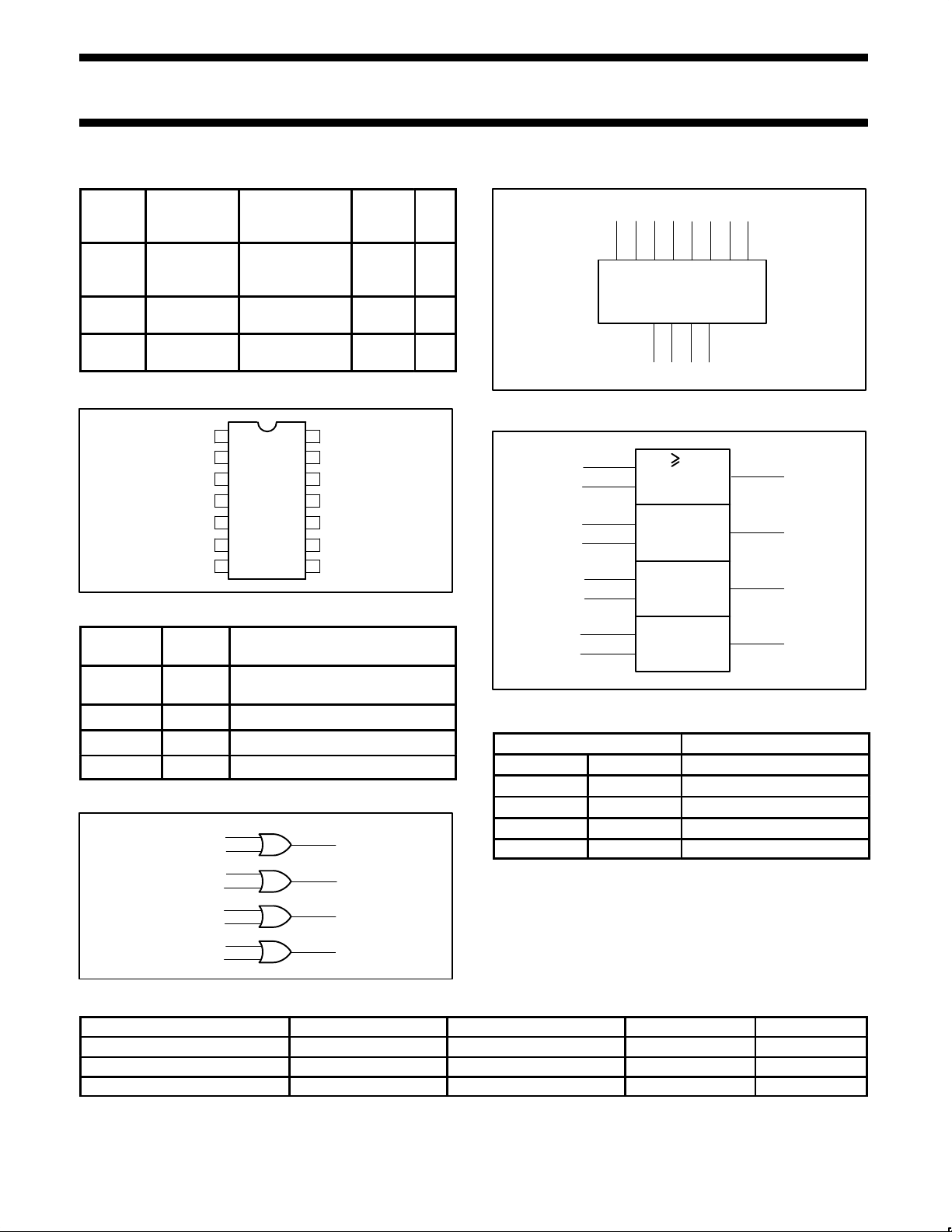
QUICK REFERENCE DATA
SYMBOL PARAMETER
CONDITIONS
T
amb
= 25°C;
GND = 0V
TYPICAL UNIT
t
PLH
t
PHL
Propagation
delay
An, Bn to Yn
CL = 50pF;
V
CC
= 3.3V
2.6
3.2
ns
C
IN
Input
capacitance
VI = 0V or 3.0V 3 pF
I
CCL
Total supply
current
Outputs Low;
V
CC
= 3.6V
1 mA
PIN CONFIGURATION
14
13
12
11
10
9
87
6
5
4
3
2
1
GND
V
CC
B2
A2
Y2
Y3
B3
A3
A0
B0
Y1
Y0
A1
B1
SA00354
PIN DESCRIPTION
PIN
NUMBER
SYMBOL NAME AND FUNCTION
1, 2, 4, 5, 9,
10, 12, 13
An, Bn Data inputs
3, 6, 8, 11 Yn Data outputs
7 GND Ground (0V)
14 V
CC
Positive supply voltage
LOGIC DIAGRAM
A0
B0
A1
B1
A2
Y0
B2
A3
B3
Y1
Y2
Y3
VCC = Pin 14
GND = Pin 7
3
6
8
11
1
2
4
5
9
10
12
13
SA00356
LOGIC SYMBOL
3 6 8 11
1 2 4 5 9 10 12 13
V
CC
= Pin 14
GND = Pin 7
SA00355
A0 B0 A1 B1 A2 B2 A3 B3
Y0 Y1 Y2 Y3
LOGIC SYMBOL (IEEE/IEC)
1
2
4
5
9
10
12
13
3
6
8
11
SF00041
1
FUNCTION TABLE
INPUTS OUTPUT
Dna Dnb Qn
L L L
L H H
H L H
H H H
NOTES:
H = High voltage level
L = Low voltage level
ORDERING INFORMATION
PACKAGES TEMPERATURE RANGE OUTSIDE NORTH AMERICA NORTH AMERICA DWG NUMBER
14-Pin Plastic SO –40°C to +85°C 74LVT32 D 74LVT32 D SOT108-1
14-Pin Plastic SSOP –40°C to +85°C 74LVT32 DB 74LVT32 DB SOT337-1
14-Pin PlasticTSSOP –40°C to +85°C 74LVT32 PW 74LVT32PW DH SOT402-1
Philips Semiconductors Product specification
74LVT323.3V Quad 2-input OR gate
1996 Aug 28
3
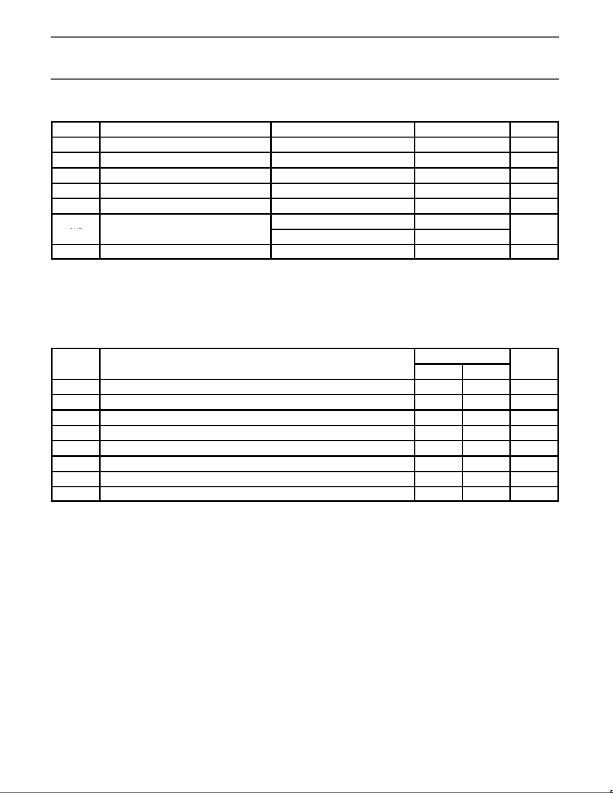
ABSOLUTE MAXIMUM RATINGS
1, 2
SYMBOL
PARAMETER CONDITIONS RATING UNIT
V
CC
DC supply voltage –0.5 to +4.6 V
I
IK
DC input diode current VI < 0 –50 mA
V
I
DC input voltage
3
–0.5 to +7.0 V
I
OK
DC output diode current VO < 0 –50 mA
V
OUT
DC output voltage
3
Output in Off or High state –0.5 to +7.0 V
Output in High state –32
I
OUT
DC output current
Output in Low state 64
mA
T
stg
Storage temperature range –65 to 150 °C
NOTES:
1. Stresses beyond those listed may cause permanent damage to the device. These are stress ratings only and functional operation of the
device at these or any other conditions beyond those indicated under “recommended operating conditions” is not implied. Exposure to
absolute-maximum-rated conditions for extended periods may affect device reliability.
2. The performance capability of a high-performance integrated circuit in conjunction with its thermal environment can create junction
temperatures which are detrimental to reliability. The maximum junction temperature of this integrated circuit should not exceed 150°C.
3. The input and output negative voltage ratings may be exceeded if the input and output clamp current ratings are observed.
RECOMMENDED OPERATING CONDITIONS
LIMITS
SYMBOL
PARAMETER
MIN MAX
UNIT
V
CC
DC supply voltage 2.7 3.6 V
V
I
Input voltage 0 5.5 V
V
IH
High-level input voltage 2.0 V
V
IL
Low-level Input voltage 0.8 V
I
OH
High-level output current –20 mA
I
OL
Low-level output current 32 mA
∆t/∆v Input transition rise or fall rate; Outputs enabled 10 ns/V
T
amb
Operating free-air temperature range –40 +85 °C
 Loading...