

Philips 74lvt273 DATASHEETS
INTEGRATED CIRCUITS
74LVT273
3.3V Octal D flip-flop
Product specification
Supersedes data of 1994 May 11
IC23 Data Handbook
1998 Feb 19
Philips Semiconductors Product specification
74L VT2733.3V Octal D flip-flop
FEA TURES
•Eight edge-triggered D-type flip-flops
•Buffered common clock
•Buffered asynchronous Master Reset
•Output capability: +64mA/–32mA
•TTL input and output switching levels
•Input and output interface capability to systems at 5V supply
•Bus-hold data inputs eliminate the need for external pull-up
resistors to hold unused inputs
•Power-up reset
•Live insertion/extraction permitted
•No bus current loading when output is tied to 5V bus
•Latchup protection exceeds 500 mA per JEDEC Std 17
•ESD protection exceeds 2000V per Mil Std 883 Method 3015 and
200V per Machine Model.
QUICK REFERENCE DATA
SYMBOL PARAMETER
t
PLH
t
PHL
C
IN
Propagation delay
CP to Qn
CL = 50pF; VCC = 3.3V
Input capacitance VI = 0V or 3.0V 4 pF
DESCRIPTION
The LVT273 is a high-performance BiCMOS product designed for
V
operation at 3.3V .
CC
This device has eight edge-triggered D-type flip-flops with individual
D inputs and Q outputs. The common buffered Clock (CP) and
Master Reset (MR
simultaneously .
The register is fully edge-triggered. The state of each D input, one
setup time before the Low-to-High clock transition, is transferred to
the corresponding flip-flop’s Q output.
All outputs will be forced Low independent of Clock or Data inputs
by a Low voltage level on the MR
applications where the true output only is required and the CP and
MR
are common elements.
CONDITIONS
T
= 25°C; GND = 0V
amb
) inputs load and reset (clear) all flip-flops
input. The device is useful for
TYPICAL UNIT
3.5
3.5
ns
ORDERING INFORMATION
PACKAGES TEMPERATURE RANGE OUTSIDE NORTH AMERICA NORTH AMERICA DWG NUMBER
20-Pin Plastic SOL –40°C to +85°C 74LVT273 D 74LVT273 D SOT163-1
20-Pin Plastic SSOP Type II –40°C to +85°C 74LVT273 DB 74LVT273 DB SOT339-1
20-Pin Plastic TSSOP Type I –40°C to +85°C 74LVT273 PW 74LVT273PW DH SOT360-1
PIN CONFIGURATION
1
MR
2
Q0
3
D0
4
D1
5
Q1
6
Q2
7
D2
8
D3
9
Q3 Q4
10 11
GND
SV00017
20
V
CC
Q7
19
D7
18
D6
17
Q6
16
Q5
15
D5
14
D4
13
12
CP
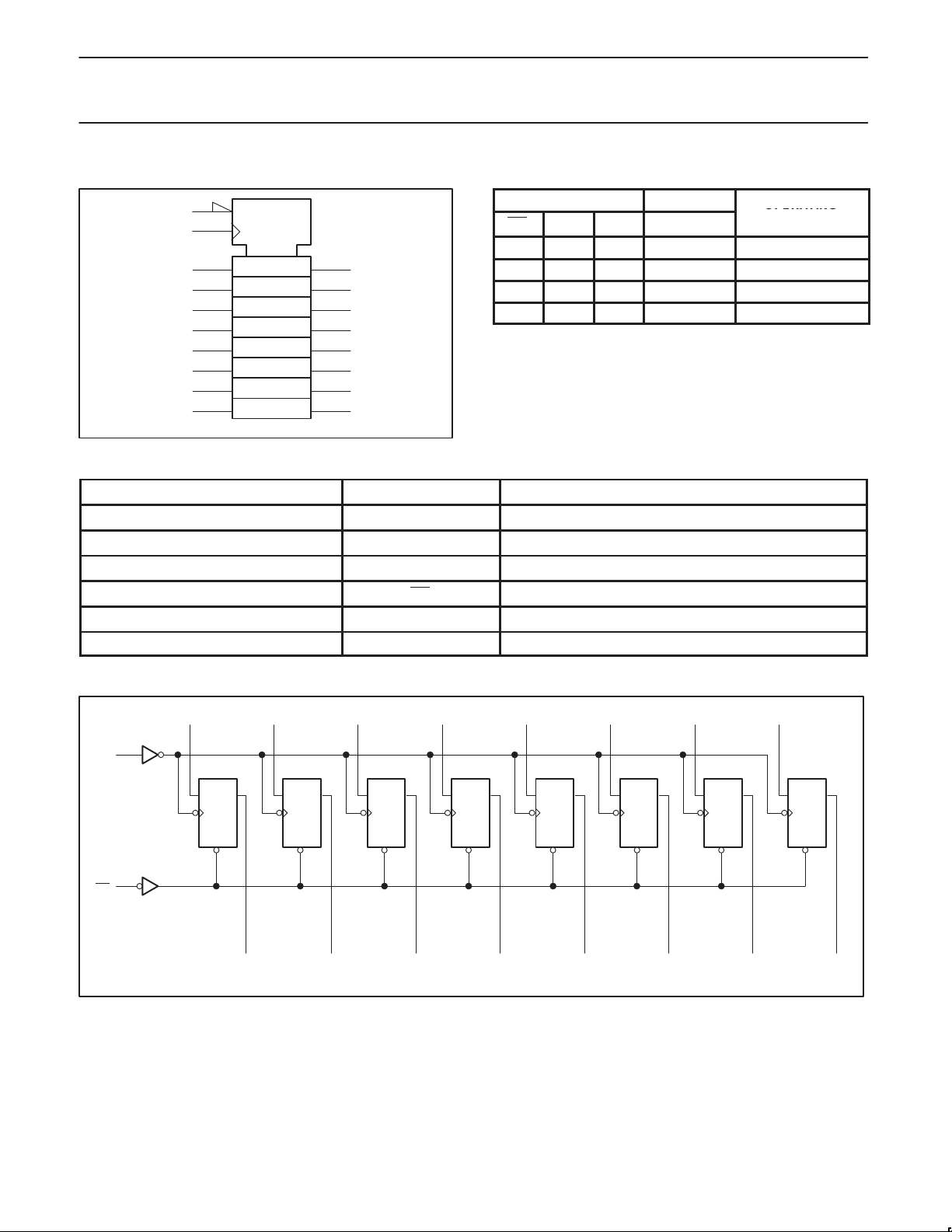
LOGIC SYMBOL
3 4 7 8 13 14 1817
D0 D1 D2 D3 D4 D5 D6 D7
CP
111MR
Q0 Q1 Q2 Q3 Q4 Q5 Q6 Q7
256912151619
SV00018
1998 Feb 19 853-1740 18985
2
Philips Semiconductors Product specification
OPERATING
74LVT2733.3V Octal D flip-flop
LOGIC SYMBOL (IEEE/IEC)
1
11
13
14
17
18
R
C1
3
1D
4
7
8
PIN DESCRIPTION
PIN NUMBER SYMBOL NAME AND FUNCTION
11 CP Clock pulse input (active rising edge)
3, 4, 7, 8, 13, 14, 17, 18 D0 – D7 Data inputs
2, 5, 6, 9, 12, 15, 16, 19 Q0 – Q7 Data outputs
1 MR Master Reset input (active-Low)
10 GND Ground (0V)
20 V
SV00019
FUNCTION TABLE
INPUTS OUTPUTS
MR CP D
Q0 – Q7
n
L X X L Reset (clear)
2
5
6
9
12
15
16
19
H ↑ h H Load “1”
H ↑ l L Load “0”
H L X Q
0
H = High voltage level
h = High voltage level one set-up time prior to the Low-to-High
clock transition
L = Low voltage level
l = Low voltage level one set-up time prior to the Low-to-High
clock transition
X = Don’t care
↑ = Low-to-High clock transition
= Output as it was
Q
0
CC
Positive supply voltage
OPERATING
MODE
Retain state
LOGIC DIAGRAM
D0
11
CP
1
MR
D1
3
Q
D
CP
R
D
Q0
4
D
CP
R
D
2
D2
7
Q
Q1
D
CP
R
D
5
D3
8
Q
Q2
D
CP
R
D
6
D4
13
Q
Q3
D
CP
R
D
9
D5
14
Q
Q4
D
CP
R
D
12
D6
17
Q
Q5
D
CP
R
D
15
D7
18
Q
16
Q6
D
CP
R
D
Q
19
Q7
SV00020
1998 Feb 19
3
Philips Semiconductors Product specification
I
DC output current
mA
SYMBOL
PARAMETER
UNIT
74LVT2733.3V Octal D flip-flop
ABSOLUTE MAXIMUM RATINGS
SYMBOL
V
CC
I
IK
V
I
I
OK
V
OUT
DC supply voltage –0.5 to +4.6 V
DC input diode current VI < 0 –50 mA
DC input voltage
DC output diode current VO < 0 –50 mA
DC output voltage
PARAMETER CONDITIONS RATING UNIT
3
3
1, 2
–0.5 to +7.0 V
output in Off or High state –0.5 to +7.0 V
Output in Low state 128
OUT
T
stg
p
Output in High State –64
Storage temperature range –65 to 150 °C
NOTES:
1. Stresses beyond those listed may cause permanent damage to the device. These are stress ratings only and functional operation of the
device at these or any other conditions beyond those indicated under “recommended operating conditions” is not implied. Exposure to
absolute-maximum-rated conditions for extended periods may affect device reliability .
2. The performance capability of a high-performance integrated circuit in conjunction with its thermal environment can create junction
temperatures which are detrimental to reliability. The maximum junction temperature of this integrated circuit should not exceed 150°C.
3. The input and output voltage ratings may be exceeded if the input and output current ratings are observed.
RECOMMENDED OPERATING CONDITIONS
LIMITS
MIN MAX
V
CC
V
V
V
I
OH
I
OL
∆t/∆v Input transition rise or fall rate; Outputs enabled 10 ns/V
T
amb
DC supply voltage 2.7 3.6 V
Input voltage 0 5.5 V
I
High-level input voltage 2.0 V
IH
Low-level Input voltage 0.8 V
IL
High-level output current –32 mA
Low-level output current 64 mA
Operating free-air temperature range –40 +85 °C
1998 Feb 19
4
 Loading...