

Philips 74LVT245PW, 74LVT245DB, 74LVT245D Datasheet

INTEGRATED CIRCUITS
74LVT245
3.3V Octal transceiver with direction pin
(3-State)
Product specification
Supersedes data of 1994 May 20
IC23 Data Handbook
1998 Feb 19
Philips Semiconductors Product specification
74L VT2453.3V Octal transceiver with direction pin (3-State)
FEA TURES
•Octal bidirectional bus interface
•3-State buffers
•Output capability: +64mA/-32mA
•TTL input and output switching levels
•Input and output interface capability to systems at 5V supply
•Bus-hold data inputs eliminate the need for external pull-up
resistors to hold unused inputs
•Live insertion/extraction permitted
•Power-up 3-State
•No bus current loading when output is tied to 5V bus
•Latch-up protection exceeds 500mA per JEDEC Std 17
•ESD protection exceeds 2000V per MIL STD 883 Method 3015
and 200V per Machine Model
QUICK REFERENCE DATA
SYMBOL PARAMETER
t
PLH
t
PHL
C
C
I
CCZ
IN
I/O
Propagation delay
An to Bn or Bn to An
Input capacitance
DIR, OE
I/O pin capacitance Outputs disabled; V
Total supply current Outputs disabled; VCC = 3.6V 0.13 mA
DESCRIPTION
The LVT245 is a high-performance BiCMOS product designed for
V
operation at 3.3V .
CC
This device is an octal transceiver featuring non-inverting 3-State
bus compatible outputs in both send and receive directions. The
control function implementation minimizes external timing
requirements. The device features an Output Enable (OE
easy cascading and a Direction (DIR) input for direction control.
T
CL = 50pF;
VCC = 3.3V
CONDITIONS
= 25°C; GND = 0V
amb
TYPICAL UNIT
2.4 ns
VI = 0V or 3.0V 4 pF
= 0V or 3.0V 10 pF
I/O
) input for
ORDERING INFORMATION
PACKAGES TEMPERATURE RANGE OUTSIDE NORTH AMERICA NORTH AMERICA DWG NUMBER
20-Pin Plastic SO –40°C to +85°C 74LVT245 D 74LVT245 D SOT163-1
20-Pin Plastic SSOP –40°C to +85°C 74LVT245 DB 74LVT245 DB SOT339-1
20-Pin Plastic TSSOP –40°C to +85°C 74LVT245 PW 74LVT245PW DH SOT360-1
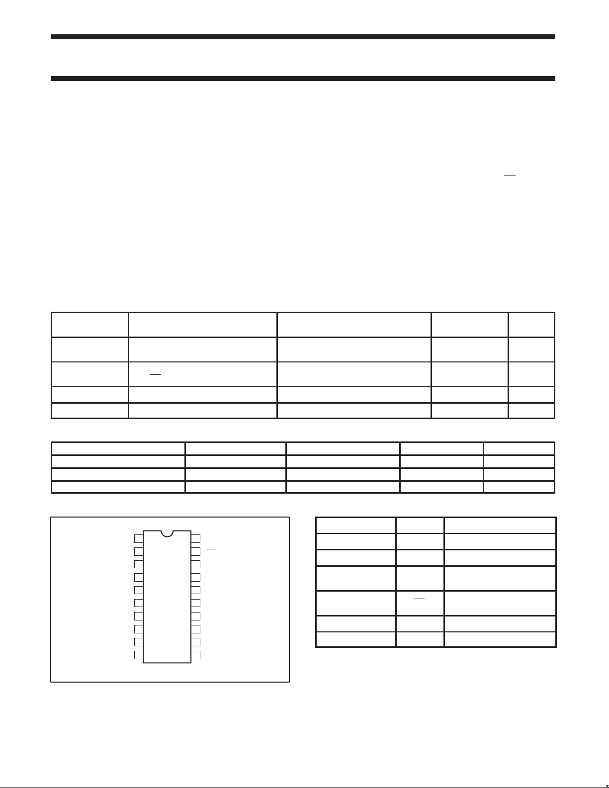
PIN CONFIGURATION
1
DIR
2
A0
3
A1
4
A2
5
A3
6
A4
7
A5
8
A6
9
A7
10 11
GND
20
19
18
17
16
15
14
13
12
SV00014
V
OE
B0
B1
B2
B3
B4
B5
B6
B7
CC
PIN DESCRIPTION
PIN NUMBER SYMBOL NAME AND FUNCTION
1 DIR Direction control input
2, 3, 4, 5, 6, 7, 8, 9 A0 – A7 Data inputs/outputs (A side)
18, 17, 16, 15, 14,
13, 12, 11
19 OE
10 GND Ground (0V)
20 V
B0 – B7 Data inputs/outputs (B side)
Output enable input
(active–Low)
CC
Positive supply voltage
1998 Feb 19 853-1727 18985
2
Philips Semiconductors Product specification
I
DC output current
mA
74LVT2453.3V Octal transceiver with direction pin (3-State)
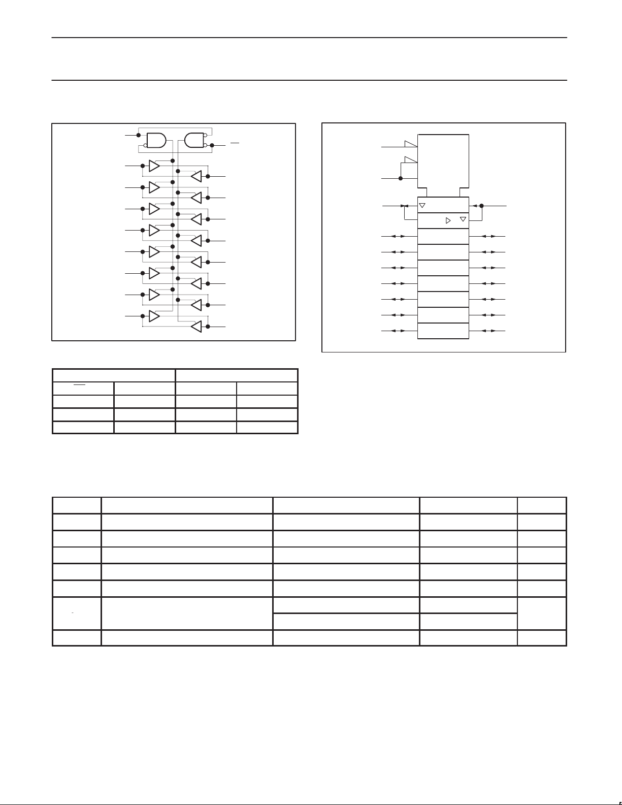
LOGIC SYMBOL
1
DIR
A0
A1
A2
A3
A4
A5
A6
A7
2
3
4
5
6
7
8
9
19
18
17
16
15
14
13
12
11
SV00016
FUNCTION TABLE
INPUTS INPUTS/OUTPUTS
OEn DIR An Bn
L L An= Bn Inputs
L H Inputs Bn =An
H X Z Z
H = High voltage level
L = Low voltage level
X = Don’t care
Z = High impedance “Off” state
OE
LOGIC SYMBOL (IEEE/IEC)
19
B0
B1
B2
B3
B4
B5
B6
B7
1
2
3
4
5
6
7
8
9
G3
3 EN1 (BA)
3 EN2 (AB)
1
18
2
17
16
15
14
13
12
11
SV00015
ABSOLUTE MAXIMUM RATINGS
SYMBOL
V
CC
I
IK
V
I
I
OK
V
OUT
DC supply voltage –0.5 to +4.6 V
DC input diode current VI < 0 –50 mA
DC input voltage
DC output diode current VO < 0 –50 mA
DC output voltage
PARAMETER CONDITIONS RATING UNIT
3
3
1,2
–0.5 to +7.0 V
Output in Off or High state –0.5 to +7.0 V
Output in Low state 128
OUT
T
stg
p
Output in High state –64
Storage temperature range –65 to +150 °C
NOTES:
1. Stresses beyond those listed may cause permanent damage to the device. These are stress ratings only and functional operation of the
device at these or any other conditions beyond those indicated under “recommended operating conditions” is not implied. Exposure to
absolute-maximum-rated conditions for extended periods may affect device reliability .
2. The performance capability of a high-performance integrated circuit in conjunction with its thermal environment can create junction
temperatures which are detrimental to reliability. The maximum junction temperature of this integrated circuit should not exceed 150°C.
3. The input and output negative voltage ratings may be exceeded if the input and output clamp current ratings are observed.
1998 Feb 19
3
 Loading...