Philips 74lvt244b DATASHEETS

INTEGRATED CIRCUITS
74LVT244B
3.3V Octal buffer/line driver (3-State)
Propduct specification
IC23 Data Handbook
1998 Nov

Philips Semiconductors Product specification
74L VT244B3.3V Octal buffer/line driver (3-State)
FEA TURES
•Octal bus interface
•3-State buffers
•Speed upgrade of 74LVTH244A
•Output capability: +64mA/-32mA
•TTL input and output switching levels
•Input and output interface capability to systems at 5V supply
•Bus-hold data inputs eliminate the need for external pull-up
resistors to hold unused inputs
•Power-up 3-State
•Live insertion/extraction permitted
•No bus current loading when output is tied to 5V bus
•Latch-up protection exceeds 500mA per JEDEC Std 17
•ESD protection exceeds 2000V per MIL STD 883 Method 3015
and 200V per Machine Model
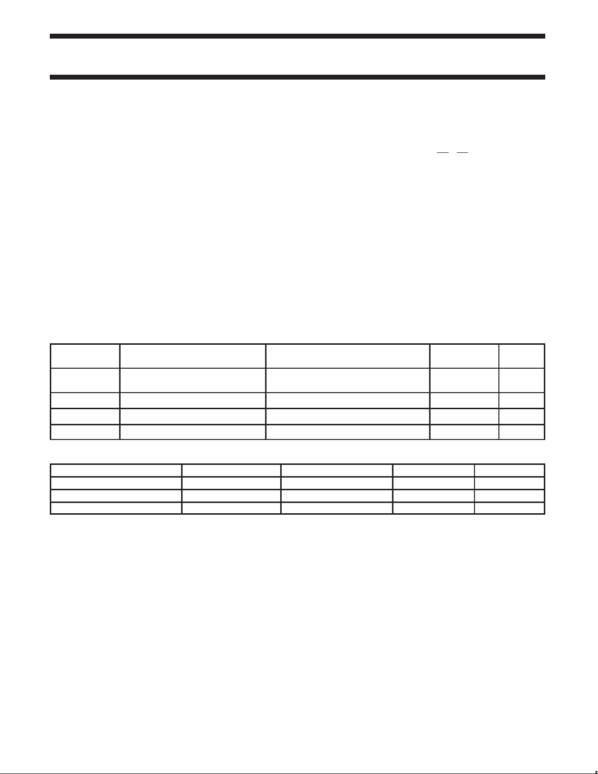
QUICK REFERENCE DATA
SYMBOL PARAMETER
C
t
PLH
t
PHL
C
OUT
I
CCZ
IN
Propagation delay
nAx to nYx
Input capacitance VI = 0V or 3.0V 4 pF
Output capacitance Outputs disabled; VO = 0V or 3.0V 8 pF
Total supply current Outputs disabled; VCC = 3.6V 0.13 mA
CL = 50pF;
VCC = 3.3V
DESCRIPTION
The LVT244B is a high-performance BiCMOS product designed for
V
operation at 3.3V .
CC
This device is an octal buffer that is ideal for driving bus lines. The
device features two Output Enables (OE
four of the 3-State outputs.
CONDITIONS
T
= 25°C; GND = 0V
amb
1, OE2), each controlling
TYPICAL UNIT
1.9
2.0
ns
ORDERING INFORMATION
PACKAGES TEMPERATURE RANGE OUTSIDE NORTH AMERICA NORTH AMERICA DWG NUMBER
20-Pin Plastic SOL –40°C to +85°C 74LVT244B D 74LVT244B D SOT163-1
20-Pin Plastic SSOP Type II –40°C to +85°C 74LVT244B DB 74LVT244B DB SOT339-1
20-Pin Plastic TSSOP Type I –40°C to +85°C 74L VT244B PW 7LVT244BPW DH SOT360-1
1998 Nov 12 853-2133 20358
2

Philips Semiconductors Product specification
74LVT244B3.3V Octal buffer/line driver (3-State)
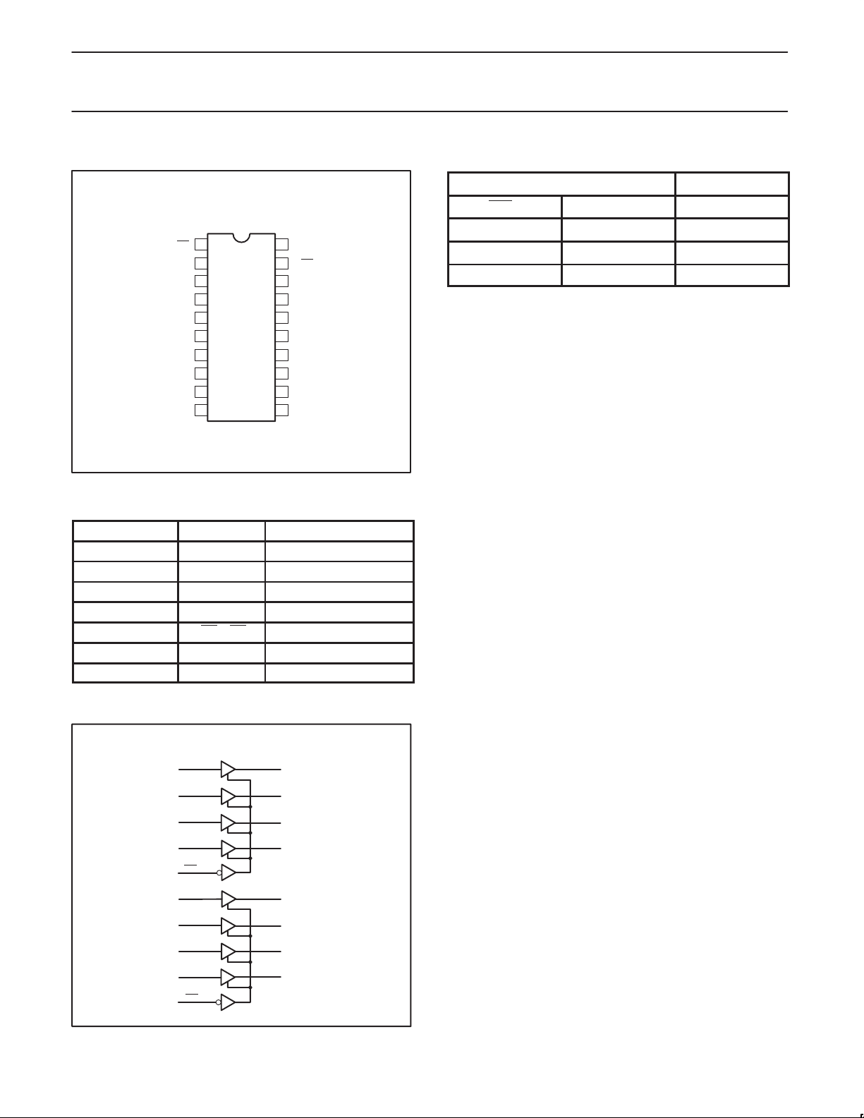
PIN CONFIGURATION
1
1OE
2
1A0
3
2Y3
4
1A1
5
2Y2
6
1A2
7
2Y1
8
1A3
9
2Y0 1Y3
10 11
GND
20
V
CC
2OE
19
1Y0
18
2A3
17
1Y1
16
2A2
15
1Y2
14
2A1
13
12
2A0
PIN DESCRIPTION
PIN NUMBER SYMBOL NAME AND FUNCTION
2, 4, 6, 8 1A0 – 1A3 Data inputs
11. 13, 15, 17 2A0 – 2A3 Data inputs
18, 16, 14, 12 1Y0 – 1Y3 Data outputs
9, 7, 5, 3 2Y0 – 2Y3 Data outputs
1, 19 1OE, 2OE Output enables
10 GND Ground (0V)
20 V
CC
Positive supply voltage
FUNCTION TABLE
INPUTS OUTPUTS
nOE1 nAx nYx
L L L
L H H
H X Z
H =High voltage level
L =Low voltage level
X = Don’t care
Z =High impedance ”off” state
SV00010
LOGIC SYMBOL
2
4
6
8
1
11
13
15
17
19
1998 Nov 12
1A0
1A1
1A2
1A3
1OE
2A0
2A1
2A2
2A3
2OE
1Y0
1Y1
1Y2
1Y3
2Y0
2Y1
2Y2
2Y3
18
16
14
12
9
7
5
3
SV00011
3
 Loading...