

Philips Semiconductors Low Voltage Products Preliminary specification
74LVT16541A3.3V ABT 16-bit buffer/driver (3-State)
1
July 1994
FEATURES
• 16-bit universal bus interface
• 3-State buffers
• Output capability: +64mA/-32mA
• TTL input and output switching levels
• Input and output interface capability to
systems at 5V supply
• Bus-hold data inputs eliminate the need for
external pull-up resistors to hold unused
inputs
• Live insertion/extraction permitted
• Power-up 3-State
• No bus current loading when output is tied
to 5V bus
• Latch-up protection exceeds 500mA per
JEDEC JC40.2 Std 17
• ESD protection exceeds 2000V per MIL
STD 883 Method 3015 and 200V per
Machine Model
DESCRIPTION
The LVT16541A is a high-performance
BiCMOS product designed for V
CC
operation
at 3.3V.
This device can be used as two octal buffers
or one 16-bit buffer. The device is ideal for
driving bus lines.
QUICK REFERENCE DATA
SYMBOL PARAMETER
CONDITIONS
T
amb
= 25°C; GND = 0V
TYPICAL UNIT
t
PLH
t
PHL
Propagation delay
nAx to nYx
CL = 50pF;
V
CC
= 3.3V
ns
C
IN
Input capacitance nOEx VI = 0V or 3.0V 4 pF
C
OUT
Output pin capacitance Outputs disabled; VO = 0V or 3.0V 10 pF
I
CCZ
Total supply current Outputs disabled; VCC = 3.6V 100 µA
ORDERING INFORMATION
PACKAGES TEMPERATURE RANGE ORDER CODE DRAWING NUMBER
48-Pin Plastic Shrink Small Outline (SSOP) Type III –40°C to +85°C 74LVT16541ADL SOT370-1
48-Pin Plastic Thin Shrink Small Outline (TSSOP) Type II –40°C to +85°C 74LVT16541ADGG SOT362-1
2 ∇
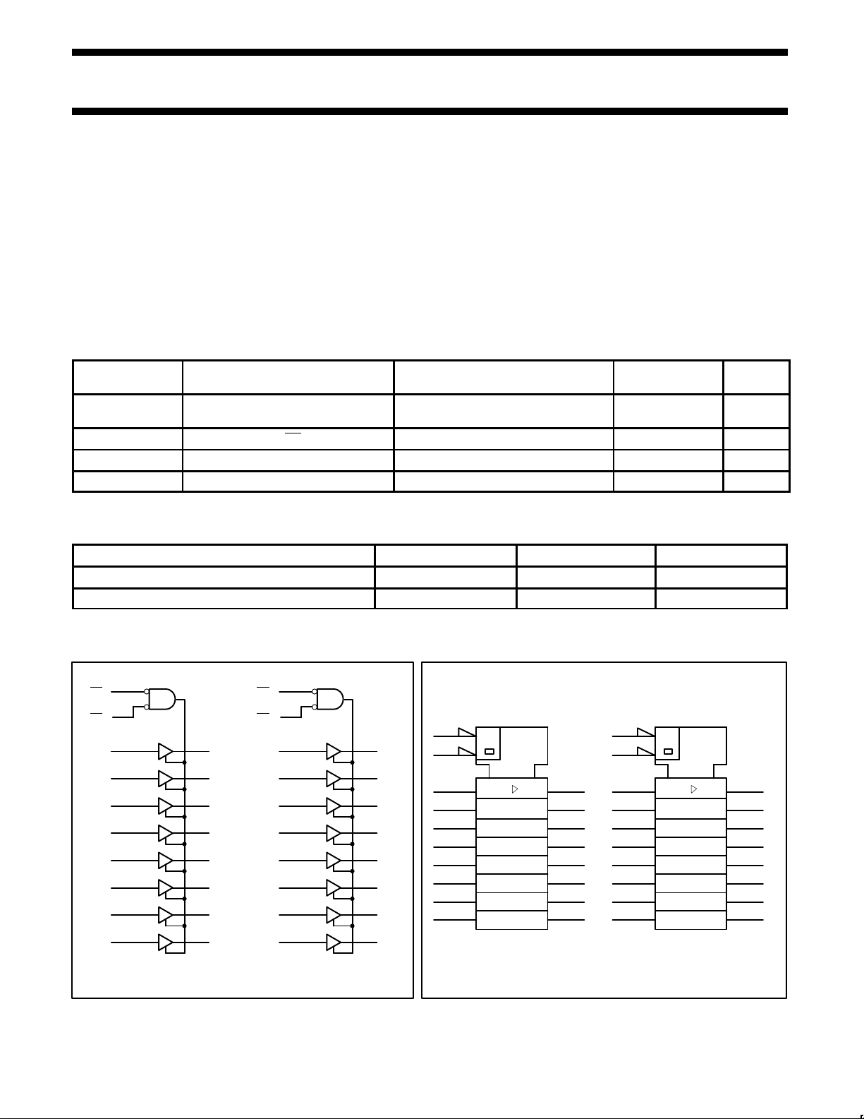
LOGIC SYMBOL
LOGIC SYMBOL (IEEE/IEC)
1
48
46
44
43
41
40
38
37
47
1OE
0
1OE
1
1A0
1A1
1A2
1A3
1A4
1A5
1A6
1A7
2
3
5
6
8
9
11
12
1Y0
1Y1
1Y2
1Y3
1Y4
1Y5
1Y6
1Y7
2OE
0
1OE
1
2Y0
24
25
36
35
33
32
30
29
27
26
2A0
2A1
2A2
2A3
2A4
2A5
2A6
2A7
13
14
16
17
19
20
22
23
2Y1
2Y2
2Y3
2Y4
2Y5
2Y6
2Y7
& EN1
1
48
47
46
44
43
41
40
38
37
2 ∇
& EN2
24
25
36
35
33
32
30
29
27
26
2
3
5
6
8
9
11
12
13
14
16
17
19
20
22
23
Philips Semiconductors Low Voltage Products Preliminary specification
74LVT16541A3.3V ABT 16-bit buffer/driver (3-State)
July 1994
2
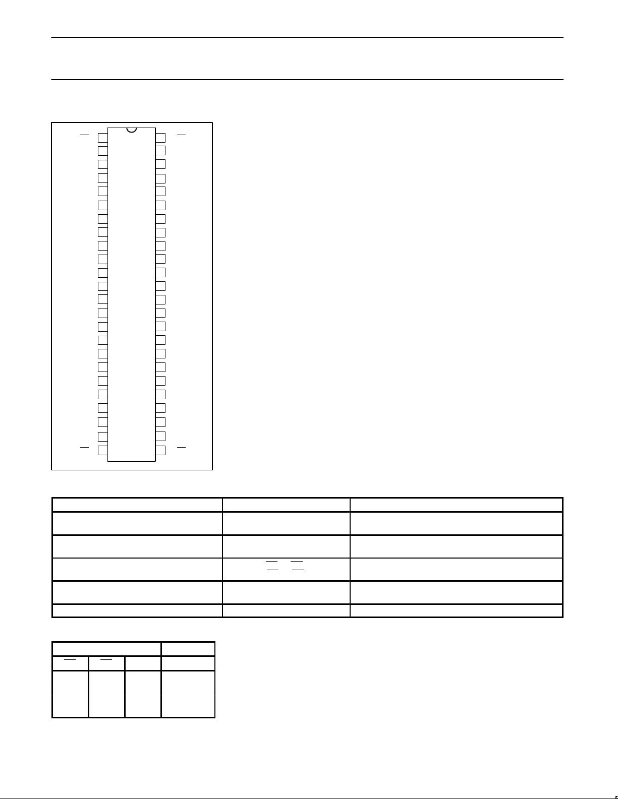
PIN CONFIGURATION
GND
GND
V
CC
V
CC
GND
GND
1OE0
1A0
1A1
1A2
1A3
1A4
1A5
1A6
1A7
2A0
2A1
2A2
2A3
2A4
2A5
2A6
2A7
2OE
0
1
2
3
4
5
6
7
8
9
10
11
12
13
14
15
16
17
18
19
20
25
26
27
28
29
30
31
32
33
34
35
36
37
38
39
40
21
22
23
24
41
42
43
44
45
46
47
48
1OE1
1Y0
1Y1
GND
1Y2
1Y3
V
CC
1Y4
1Y5
GND
1Y6
1Y7
2Y0
2Y1
GND
2Y2
2Y3
V
CC
2Y4
2Y5
GND
2Y6
2Y7
2OE
1
PIN DESCRIPTION
PIN NUMBER SYMBOL NAME AND FUNCTION
47, 46, 44, 43, 41, 40, 38, 37,
36, 35, 33, 32, 30, 29, 27, 26
1A0–1A7
2A0–2A7
Data inputs
2, 3, 5, 6, 8, 9, 11, 12,13,
14, 16, 17, 19, 20, 22, 23
1Y0–1Y7
2Y0–2Y7
Data outputs
1, 48
24, 25
1OE0, 1OE1,
2OE
0, 2OE1
Output enables
4, 10, 15, 21,
28, 34, 39, 45
GND Ground (0V)
7, 18, 31, 42 V
CC
Positive supply voltage
FUNCTION TABLE
INPUTS OUTPUTS
nOE0 nOE1 nAx nYx
L L L L
L L H H
X H X Z
H X X Z
H = High voltage level
L = Low voltage level
X = Don’t care
Z = High Impedance “off” state
 Loading...