

Philips 74lvt16244b DATASHEETS
INTEGRATED CIRCUITS
74LVT16244B
3.3V LVT 16-bit buffer/driver (3-State)
Prooduct specification
Supersedes data of 1998 Feb 19
IC23 Data Handbook
1998 Oct 07
Philips Semiconductors Product specification
74L VT16244B3.3V 16-bit buffer/driver (3-State)
FEA TURES
•16-bit bus interface
•3-State buffers
•Output capability: +64mA/-32mA
•TTL input and output switching levels
•Input and output interface capability to systems at 5V supply
•Bus-hold data inputs eliminate the need for external pull-up
resistors to hold unused inputs
•Live insertion/extraction permitted
•Power-up 3-State
•No bus current loading when output is tied to 5V bus
•Latch-up protection exceeds 500mA per JEDEC Std 17
•ESD protection exceeds 2000V per MIL STD 883 Method 3015
and 200V per Machine Model
QUICK REFERENCE DATA
SYMBOL PARAMETER
C
t
PLH
t
PHL
C
OUT
I
CCZ
IN
Propagation delay
nAx to nYx
Input capacitance nOE VI = 0V or 3.0V 3 pF
Output capacitance Outputs disabled; VO = 0V or 3.0V 9 pF
Total supply current Outputs disabled; VCC = 3.6V 70 µA
CL = 50pF;
V
= 3.3V
CC
DESCRIPTION
The 74LVT16244B is a high-performance BiCMOS product
designed for V
This device is a 16-bit buffer and line driver featuring non-inverting
3-State bus outputs. The device can be used as four 4-bit buffers,
two 8-bit buffers, or one 16-bit buffer.
CONDITIONS
T
amb
operation at 3.3V .
CC
= 25°C
TYPICAL UNIT
1.8 ns
ORDERING INFORMATION
PACKAGES TEMPERATURE RANGE OUTSIDE NORTH AMERICA NORTH AMERICA DWG NUMBER
48-Pin Plastic SSOP Type III –40°C to +85°C 74LVT16244B DL VT16244B DL SOT370-1
48-Pin Plastic TSSOP Type II –40°C to +85°C 74LVT16244B DGG VT16244B DGG SOT362-1
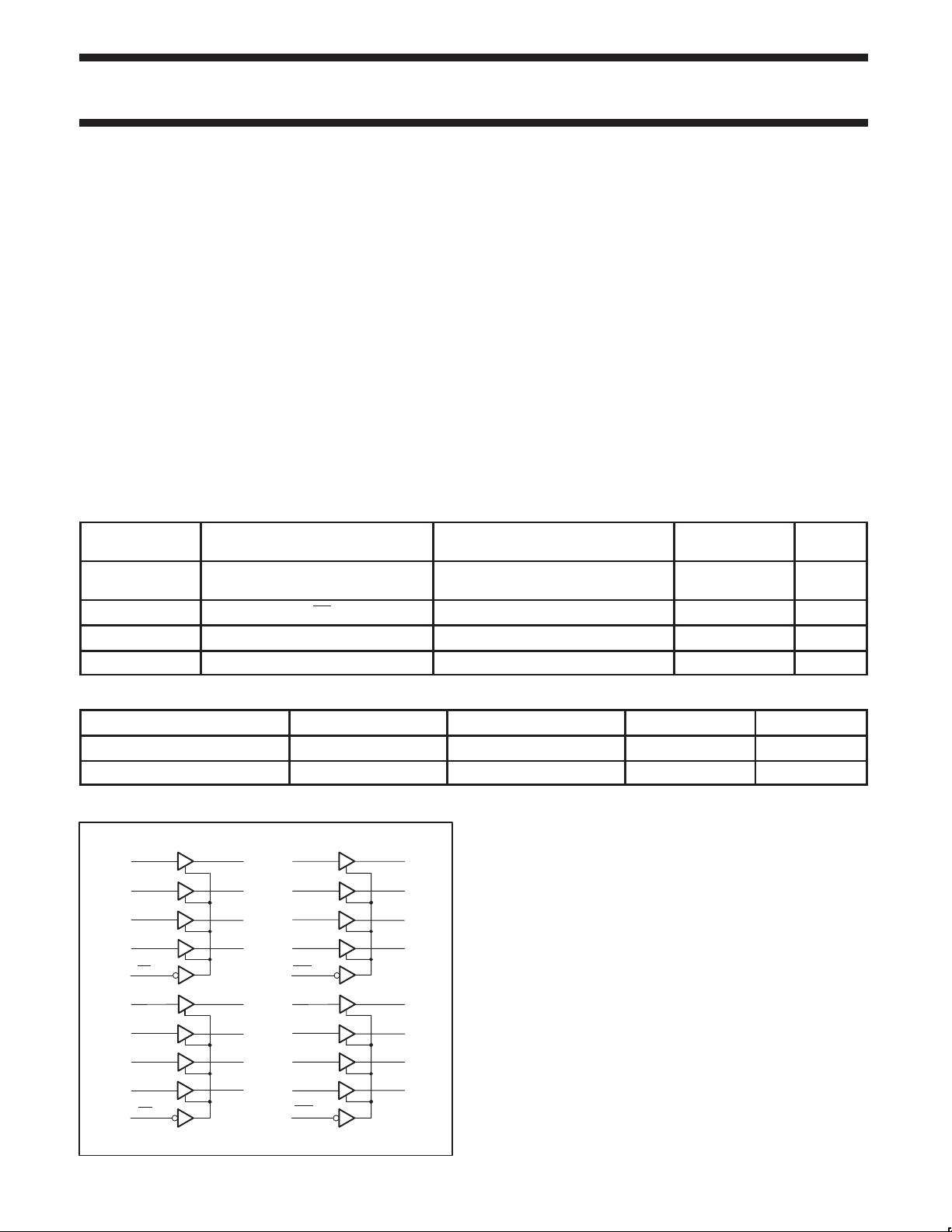
LOGIC SYMBOL
1A0
47
1A1
46
1A2
44
1A3
43
1OE
1
2A0
41
2A1
40
2A2
38
2A3
37
2OE
48
1Y0
1Y1
1Y2
1Y3
2Y0
2Y1
2Y2
2Y3
3A0
36
2
3A1
3
35
3A2
33
5
3A3
32
6
3OE
25
4A0
8
30
4A1
9
29
4A2
11
27
4A3
26
12
4OE
24
3Y0
3Y1
3Y2
3Y3
4Y0
4Y1
4Y2
4Y3
SA00014
13
14
16
17
19
20
22
23
1998 Oct 07 853-1778 20144
2
Philips Semiconductors Product specification
74LVT16244B3.3V 16-bit buffer/driver (3-State)
LOGIC SYMBOL (IEEE/IEC)
1OE
2OE
3OE
4OE
1A1
1A2
1A3
1A4
2A1
2A2
2A3
2A4
3A1
3A2
3A3
3A4
4A1
4A2
4A3
4A4
1
48
25
24
47
46
44
43
41
40
38
37
36
35
33
32
30
29
27
26
EN1
EN2
EN3
EN4
PIN CONFIGURATION
1
1OE
2
1Y0
3
1Y1
4
GND
5
1Y2
6
1Y3
7
V
CC
8
2Y0
9
2Y1
10
GND
11
2Y2
12
2Y3
13
3Y0
14
3Y1
15
GND
16
3Y2
17
3Y4
18
V
CC
19
4Y0
20
4Y1
21
GND
22
4Y2
23
4Y3
24
4OE
PIN DESCRIPTION
PIN NUMBER SYMBOL NAME AND FUNCTION
47, 46, 44, 43
41, 40, 38, 37
36, 35, 33, 32
30, 29, 27, 26
2
1 ∇
1
2 ∇1
3 ∇1
4 ∇1
1Y1
3
1Y2
5
1Y3
6
1Y4
8
2Y1
9
2Y2
11
2Y3
12
2Y4
13
3Y1
14
3Y2
16
3Y3
17
3Y4
19
4Y1
20
4Y2
22
4Y3
23
4Y4
SA00019
2, 3, 5, 6
8, 9, 11, 12
13, 14, 16, 17
19, 20, 22, 23
1, 48
25, 24
4, 10, 15, 21
28, 34, 39, 45
7, 18, 31, 42 V
FUNCTION TABLE
nOE nAx nYx
L L L
L H H
H X Z
H = High voltage level
L = Low voltage level
X = Don’t care
48
2OE
47
1A0
46
1A1
45
GND
44
1A2
43
1A3
42
V
CC
41
2A0
40
2A1
39
GND
38
2A2
37
2A3
36
3A0
35
3A1
34
GND
33
3A2
32
3A3
V
31
CC
30
4A0
29
4A1
28
GND
27
4A2
26
4A3
25
3OE
Z = High Impedance “off” state
1A0 - 1A3,
2A0 - 2A3,
3A0 - 3A3,
Data inputs
4A0 - 4A3
1Y0 - 1Y3,
2Y0 - 2Y3,
3Y0 - 3Y3,
Data outputs
4Y0 - 4Y3
1OE, 2OE,
3OE, 4OE
Output enables
GND Ground (0V)
CC
Positive supply voltage
INPUTS OUTPUTS
1998 Oct 07
SA00013
3
 Loading...