

Philips 74LVCH32374A Datasheet

INTEGRATED CIRCUITS
DATA SH EET
74LVCH32374A
32-bit edge-triggered D-type
flip-flop with 5 V tolerant
inputs/outputs; 3-state
Product specification
File under Integrated Circuits, IC24
1999 Nov 24

Philips Semiconductors Product specification
32-bit edge-triggered D-type flip-flop with
5 V tolerant inputs/outputs; 3-state
FEATURES
• 5 V tolerant inputs/outputs for interfacing with 5 V logic
• Wide supply voltage range from 1.2 to 3.6 V
• CMOS low power consumption
• MULTIBYTE flow-trough standardpin-out architecture
• Low inductance multiple power and ground pins for
minimum noise and ground bounce
• Direct interface with TTL levels
• Bus hold on data inputs
• Typical output ground bounce voltage:
V
<0.8VatVCC= 3.3 V and T
OLP
amb
=25°C
• Typical output undershoot voltage:
V
>2VatVCC= 3.3 V and T
OHV
amb
=25°C
• Power off disables outputs, permitting live insertion
• Packaged in plastic fine-pitch ball grid array package.
DESCRIPTION
The 74LVCH32374A is a high-performance, low-power,
low-voltage, Si-gate CMOS device, superior to most
advanced CMOS compatible TTL families.
The inputs can be driven from either 3.3 or 5 V devices. In
3-state operation, the outputs can handle 5 V. These
features allow the use of these devices in a mixed
3.3 or 5 V environment.
The 74LVCH32374A is a 32-bit edge-triggered flip-flop
featuring separate D-type inputs for each flip-flop and
3-state outputs for bus oriented applications. The
74LVCH32374A consists of 4 sections of eight
edge-triggered flip-flops. A clock (nCP) input and an
output enable input (nOE) are provided per 8-bit section.
The flip-flops willstore the state of theirindividual D-inputs
that meet the set-up and hold time requirements on the
LOW-to-HIGH nCP transition.
When input nOE is LOW, the contents of the flip-flops are
available at the outputs. When input nOE is HIGH, the
outputs go tothe high-impedance OFF-state. Operation of
the nOE input does not affect the state of the flip-flops.
74LVCH32374A
The 74LVCH32374A bus hold data input circuitseliminate
the need for external pull-up resistors to hold unused
inputs.
QUICK REFERENCE DATA
GND = 0 V; T
=25°C; tr=tf≤2.5 ns
amb
SYMBOL PARAMETER CONDITIONS TYPICAL UNIT
t
PHL/tPLH
f
max
C
I
C
PD
propagation delay nCP to nQ
n
maximum clock frequency 150 MHz
input capacitance 5.0 pF
power dissipation capacitance per
CL= 50 pF; VCC= 3.3 V 3.8 ns
VI= GND to VCC; note 1 30 pF
buffer
Note
1. C
is used to determine the dynamic power dissipation (PDin µW).
PD
PD=CPD× V
2
× fi+ Σ (CL× V
CC
2
× fo) where:
CC
fi= input frequency in MHz;
fo= output frequency in MHz;
CL= output load capacitance in pF;
VCC= supply voltage in Volts;
Σ (CL× V
2
× fo) = sum of the outputs.
CC
1999 Nov 24 2

Philips Semiconductors Product specification
32-bit edge-triggered D-type flip-flop with
74LVCH32374A
5 V tolerant inputs/outputs; 3-state
FUNCTION TABLE
See note 1.
OPERATING MODE
Load and read register L ↑ lLL
Load register and disable
outputs
Note
1. H = HIGH voltage level;
h = HIGH voltage level one set-up time prior to the HIGH-to-LOW CP transition;
L = LOW voltage level;
l = LOW voltage level one set-up time prior to the HIGH-to-LOW CP transition;
Z = high-impedance OFF-state;
↑ = LOW-to-HIGH CP transition.
OE nCP nD
n
L↑hHH
H ↑ lLZ
H↑hHZ
INPUTS
n
INTERNAL
FLIP-FLOPS
OUTPUTS
nQ
n
ORDERING INFORMATION
TYPE NUMBER
74LVCH32374AEC −40 to +85 °C 96 LFBGA96 plastic SOT536-1
PINNING
SYMBOL DESCRIPTION
nD
n
nCP clock inputs
nQ
n
GND ground (0 V)
n
OE output enable inputs (active LOW)
V
CC
TEMPERATURE RANGE PINS PACKAGE MATERIAL CODE
data inputs
flip-flop outputs
DC supply voltage
PACKAGE
1999 Nov 24 3
Philips Semiconductors Product specification
32-bit edge-triggered D-type flip-flop with
5 V tolerant inputs/outputs; 3-state
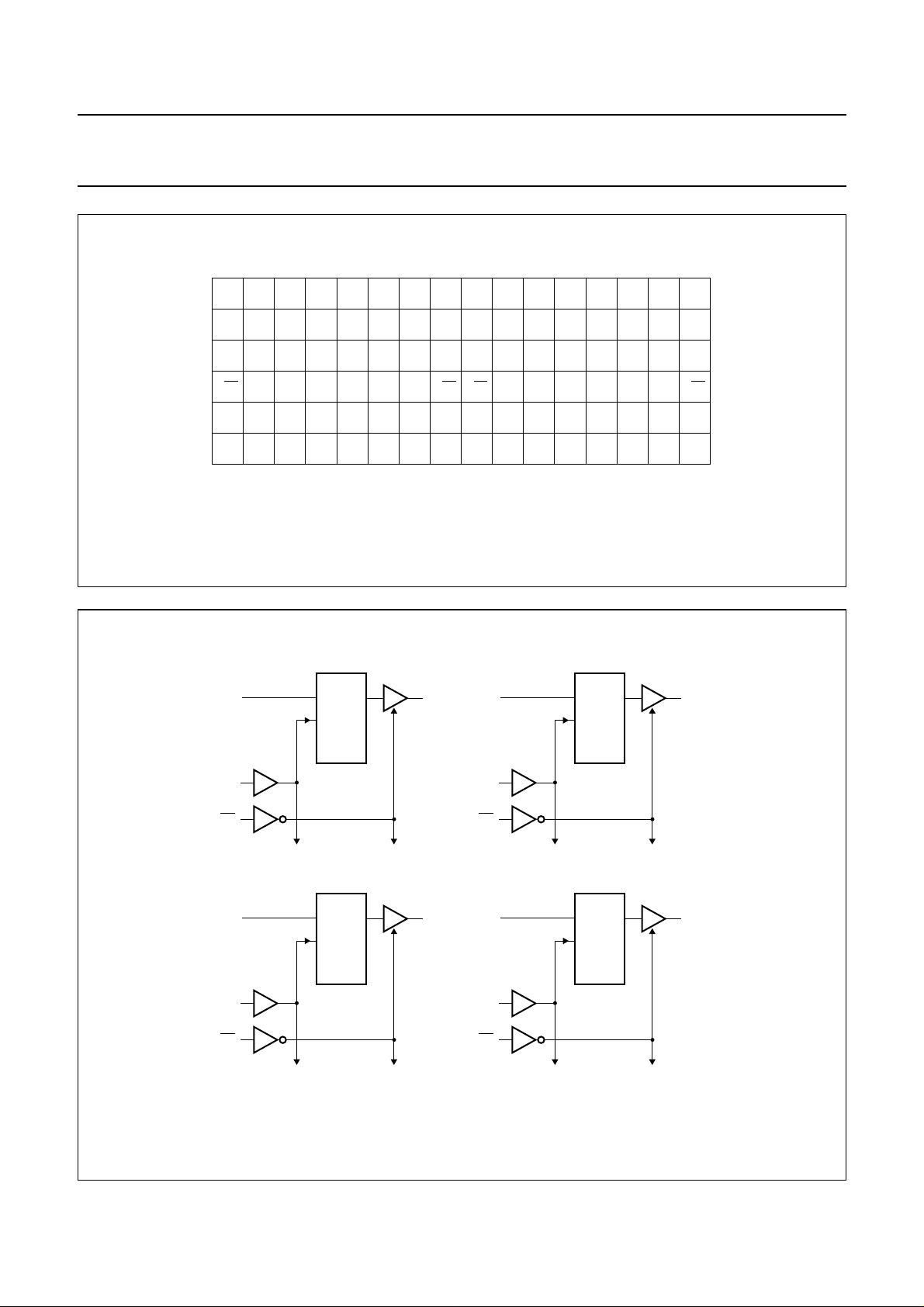
handbook, full pagewidth
6
1D11D31D51D72D12D32D52D73D13D33D53D74D14D34D54D
5
1D01D21D41D62D02D22D42D63D03D23D43D64D04D24D44D
1CP 2CP 3CPGND GND GND GND 4CPV
4
1OE
3 2OE 3OEGND GND GND GND 4OEV
1Q01Q21Q41Q62Q02Q22Q42Q63Q03Q23Q43Q64Q04Q24Q44Q
2
1Q11Q31Q51Q72Q12Q32Q52Q73Q13Q33Q53Q74Q14Q34Q54Q
1
AHJBDEG TCF KMNRLP
CC
CC
V
CC
V
CC
Fig.1 Pin configuration.
GND GND GND GNDV
GND GND GND GNDV
CC
CC
74LVCH32374A
MNA497
6
7
V
CC
V
CC
7
6
handbook, full pagewidth
1D
1CP
1OE
3D
3CP
3OE
0
0
DQ
CP CP
FF 1
to 7 other channels
DQ
CP CP
FF 17
to 7 other channels
1Q
3Q
2D
2CP
2OE
4D
4CP
4OE
0
0
0
0
DQ
FF 9
to 7 other channels
D
Q
FF 25
to 7 other channels
2Q
0
4Q
0
MNA498
Fig.2 Logic symbol.
1999 Nov 24 4

Philips Semiconductors Product specification
32-bit edge-triggered D-type flip-flop with
5 V tolerant inputs/outputs; 3-state
data
input
V
CC
handbook, halfpage
74LVCH32374A
to internal circuit
MNA473
Fig.3 Bus hold circuit.
1999 Nov 24 5
 Loading...