

Philips 74LVCH322244A, 74LVC322244A Datasheet

DATA SH EET
Product specification
File under Integrated Circuits, IC24
1999 Aug 31
INTEGRATED CIRCUITS
74LVC322244A; 74LVCH322244A
32-bit buffer/line driver; with 30 Ω
series termination resistors; 5 V
input/output tolerant; 3-state
1999 Aug 31 2
Philips Semiconductors Product specification
32-bit buffer/line driver; with 30 Ω series termination
resistors; 5 V input/output tolerant; 3-state
74LVC322244A;
74LVCH322244A
FEATURES
• 5 V tolerant inputs/outputs for interfacing with 5 V logic
• Wide supply voltage range of 1.2 to 3.6 V
• CMOS low power consumption
• MULTIBYTE flow-trough standardpin-out architecture
• Low inductance multiple power and ground pins for
minimum noise and ground bounce
• Direct interface with TTL levels
• Bus hold on data inputs (74LVCH322244A only)
• Integrated 30 Ω termination resistors
• Typical output ground bounce voltage:
V
OLP
<0.8 V at VCC= 3.3 V; T
amb
=25°C
• Typical output VOH undershoot voltage:
V
OHV
>2VatVCC= 3.3 V; T
amb
=25°C
• Power-off disabled outputs, permitting live insertion
• Plastic fine-pitch ball grid array package.
DESCRIPTION
The74LVC(H)322244Aisahigh-performance,low-power,
low-voltage, Si-gate CMOS device, superior to most
advanced CMOS compatible TTL families. Inputs can be
driven from either 3.3 or 5 V devices. In 3-state operation,
outputs can handle 5 V. These features allow the use of
these devices in a mixed 3.3 and 5 V environment.
The74LVC(H)322244Ais a 32-bit non-inverting buffer/line
driver with 3-state outputs. The 3-state outputs are
controlled by the output enable inputs 1OE and 2OE.
A HIGH on input nOE causes the outputs to assume a
high-impedance OFF-state.
The 74LVC(H)322244A is designed with 30 Ω series
terminationresistors in bothHIGH and LOW outputstages
to reduce line noise.
To ensure the high-impedance state during power-up or
power-down, input nOE should be tied to VCC through a
pull-up resistor; the minimum value of the resistor is
determined by the current-sinking capability of the driver.
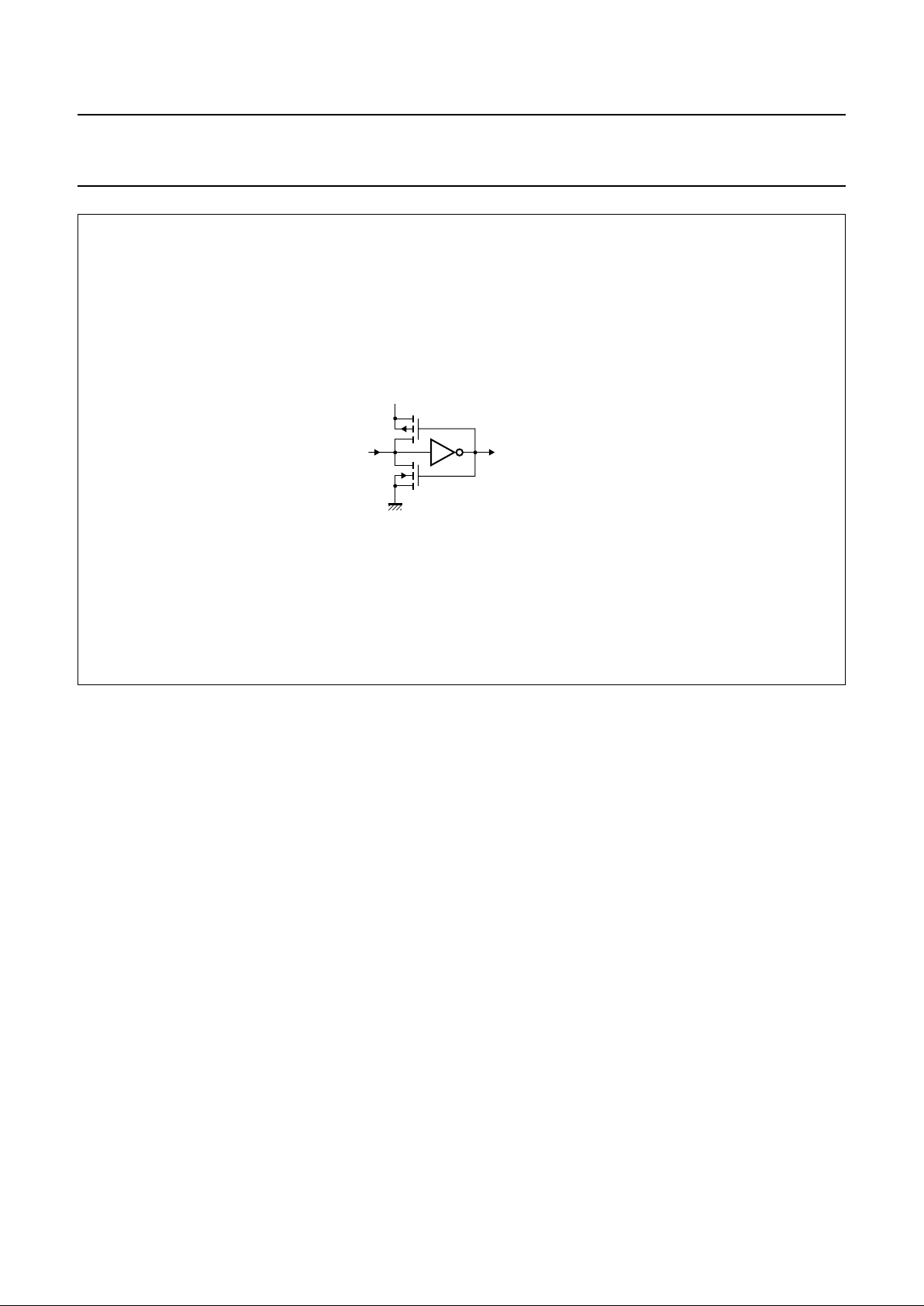
The 74LVCH322244A bus hold data input circuit
eliminates the need for external pull-up resistors to hold
unused or floating data inputs at a valid logic level (see
Fig.3).
QUICK REFERENCE DATA
Ground = 0 V; T
amb
=25°C; tr=tf≤2.5 ns.
Note
1. C
PD
is used to determine the dynamic power dissipation (PDin µW).
PD=CPD× V
CC
2
× fi+ Σ(CL× V
CC
2
× fo) where:
fi= input frequency in MHz;
fo= output frequency in MHz;
C
L
= output load capacitance in pF;
VCC= supply voltage in Volts;
Σ(CL× V
CC
2
× fo) = sum of the outputs.
SYMBOL PARAMETER CONDITIONS TYPICAL UNIT
t
PHL/tPLH
propagation delay nAnto nY
n
CL= 50 pF; VCC= 3.3 V 2.9 ns
C
I
input capacitance 5.0 pF
C
PD
power dissipation capacitance per
buffer
VI= GND to VCC; note 1 25 pF
1999 Aug 31 3
Philips Semiconductors Product specification
32-bit buffer/line driver; with 30 Ω series termination
resistors; 5 V input/output tolerant; 3-state
74LVC322244A;
74LVCH322244A
FUNCTION TABLE
See note 1.
Note
1. H = HIGH voltage level;
L = LOW voltage level;
X = don’t care;
Z = high-impedance OFF-state.
ORDERING INFORMATION
PINNING
INPUT OUTPUT
n
OE nA
n
nY
n
LLL
LHH
HXZ
TYPE NUMBER
PACKAGES
TEMPERATURE
RANGE
PINS PACKAGE MATERIAL CODE
74LVC322244AEC −40 to +85 °C 96 LFBGA96 plastic SOT536-1
74LVCH322244AEC 96 LFBGA96 plastic SOT536-1
SYMBOL DESCRIPTION
nA
n
data inputs
nY
n
data outputs
GND ground (0 V)
nOE 3-state output enable inputs (active LOW)
V
CC
DC supply voltage
1999 Aug 31 4
Philips Semiconductors Product specification
32-bit buffer/line driver; with 30 Ω series termination
resistors; 5 V input/output tolerant; 3-state
74LVC322244A;
74LVCH322244A
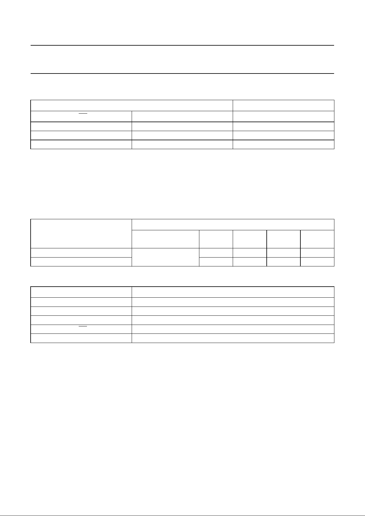
handbook, full pagewidth
MNA471
1A11A32A12A33A13A34A14A25A15A36A16A37A17A38A18A
2
1A01A22A02A23A03A24A04A35A05A26A06A27A07A28A08A
3
1Y01Y22Y02Y23Y03Y24Y04Y35Y05Y26Y06Y27Y07Y28Y08Y
3
1Y11Y32Y12Y33Y13Y34Y14Y25Y15Y36Y16Y37Y17Y38Y18Y
2
2OE 3OE 6OEGND GND GND GND 7OEV
CC
V
CC
GND GND GND GNDV
CC
V
CC
1OE
6
5
2
1
4
3 4OE 5OEGND GND GND GND 8OEV
CC
V
CC
GND GND GND GNDV
CC
V
CC
AHJBDEG TCF KMNRLP
Fig.1 Pin configuration.
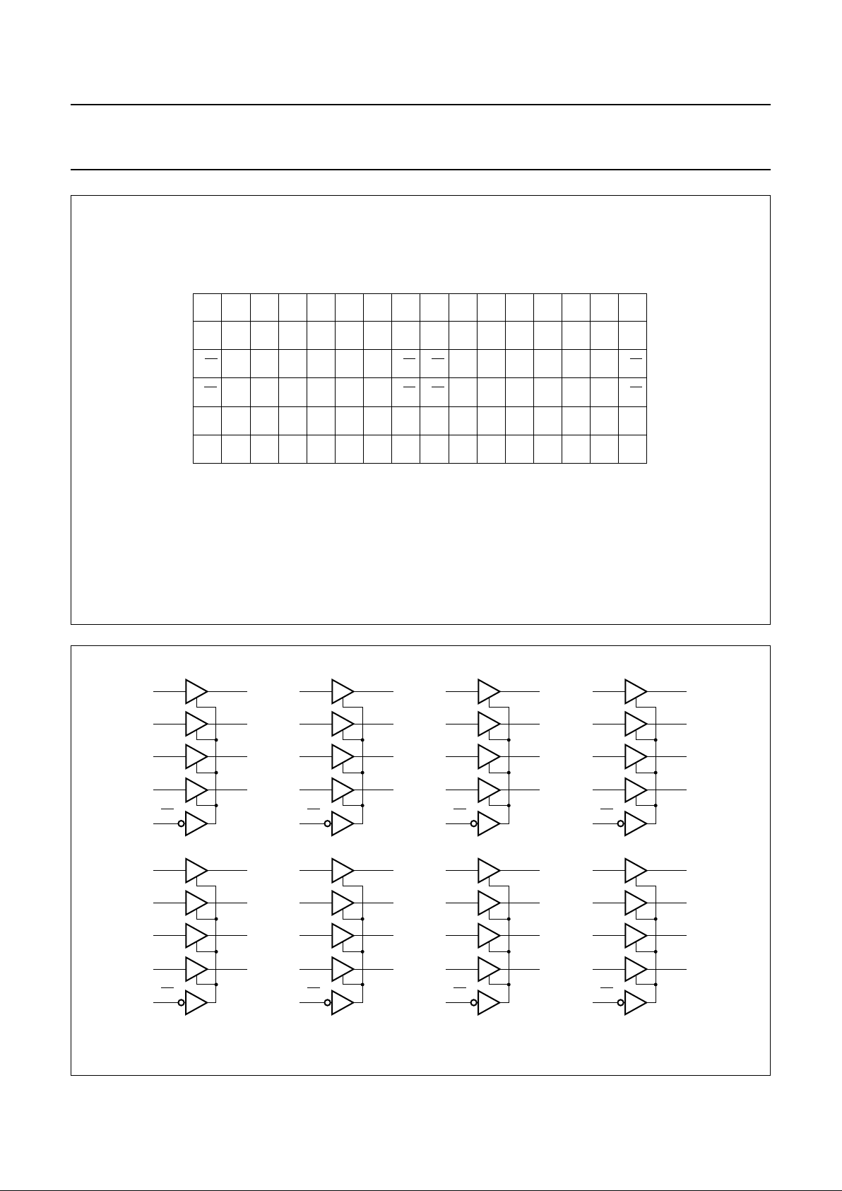
Fig.2 Logic symbol.
handbook, full pagewidth
A3
B6
B5
A6
A5
1A
3
1A
2
1A
1
1A
0
A2
A1
B2
B1
1Y
0
1Y
1
1Y
2
1Y
3
1OE
H4
F6
F5
E6
E5
3A
3
3A
2
3A
1
3A
0
E2
E1
F2
F1
3Y
0
3Y
1
3Y
2
3Y
3
3OE
J3
K6
K5
J6
J5
5A
3
5A
2
5A
1
5A
0
J2
J1
K2
K1
5Y
0
5Y
1
5Y
2
5Y
3
5OE
T4
P6
P5
N6
N5
7A
3
7A
2
7A
1
7A
0
N2
N1
P2
P1
7Y
0
7Y
1
7Y
2
7Y
3
7OE
A4
D6
D5
C6
C5
2A
3
2A
2
2A
1
2A
0
C2
C1
D2
D1
2Y
0
2Y
1
2Y
2
2Y
3
2OE
H3
H5
H6
G6
G5
4A
3
4A
2
4A
1
4A
0
G2
G1
H1
H2
4Y
0
4Y
1
4Y
2
4Y
3
4OE
J4
M6
M5
L6
L5
6A
3
6A
2
6A
1
6A
0
L2
L1
M2
M1
6Y
0
6Y
1
6Y
2
6Y
3
6OE
MNA472
T3
T5
T6
R6
R5
8A
3
8A
2
8A
1
8A
0
R2
R1
T1
T2
8Y
0
8Y
1
8Y
2
8Y
3
8OE
1999 Aug 31 5
Philips Semiconductors Product specification
32-bit buffer/line driver; with 30 Ω series termination
resistors; 5 V input/output tolerant; 3-state
74LVC322244A;
74LVCH322244A
Fig.3 Bus hold circuit.
handbook, halfpage
MNA473
V
CC
data
input
to internal circuit
 Loading...