

Philips 74LVCH245APW, 74LVC245APW, 74LVC245ADB, 74LVC245AD, 74LVCH245AD Datasheet

INTEGRATED CIRCUITS
74LVC245A/74LVCH245A
Octal bus transceiver with direction pin
with 5-volt tolerant inputs/outputs
(3-State)
Product specification
Supersedes data of 1997 Dec 19
IC24 Data Handbook
1998 May 20
Philips Semiconductors Product specification
Octal bus transceiver with direction pin with
5-volt tolerant inputs/outputs (3-State)
FEA TURES
•5-volt tolerant inputs/outputs, for interfacing with 5-volt logic
•Supply voltage range of 2.7V to 3.6V
•Complies with JEDEC standard no. 8-1A
•CMOS low power consumption
•Direct interface with TTL levels
•High impedance when V
CC
= 0V
•Bushold on all data inputs (74LVCH245A only)
DESCRIPTION
The 74LVC245A/74LVCH245A is a high-performance, low-power,
low-voltage, Si-gate CMOS device, superior to most advanced
CMOS compatible TTL families.
Inputs can be driven from either 3.3V or 5V devices. In 3-State
operation, outputs can handle 5V. These features allow the use of
these devices as translators in a mixed 3.3V/5V environment.
The 74LVC245A/74LVCH245A is an octal transceiver featuring
non-inverting 3-State bus compatible outputs in both send and
receive directions. The ’245’ features an output enable (OE
easy cascading and a send/receive (DIR) input for direction control.
OE
The ’245’ is functionally identical to the ’640’, but the ’640’ has true
(non-inverting) outputs.
controls the outputs so that the buses are effectively isolated.
74L VC245A
74L VCH245A
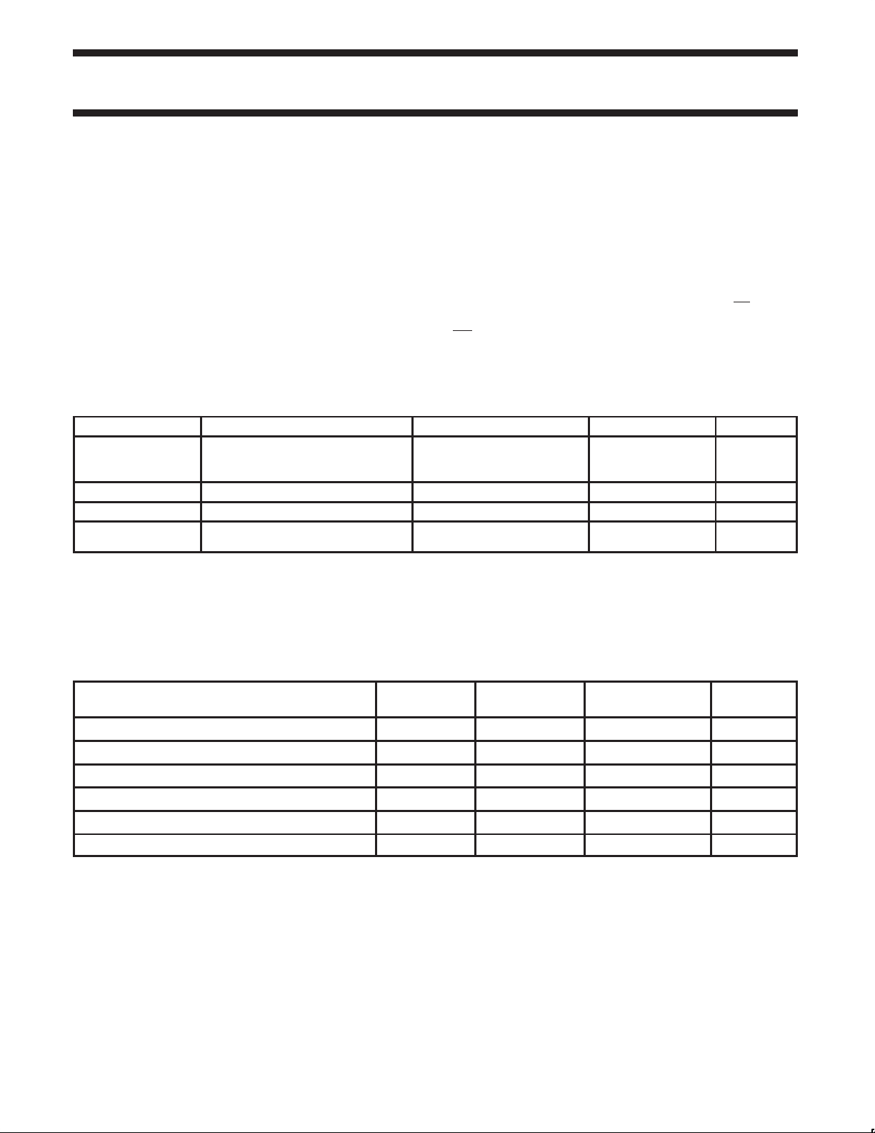
QUICK REFERENCE DATA
SYMBOL PARAMETER CONDITIONS TYPICAL UNIT
Propagation delay
t
PHL/tPLH
C
I
C
I/O
C
PD
NOTE:
is used to determine the dynamic power dissipation (PD in W):
1. C
PD
= CPD x V
P
D
= input frequency in MHz; CL = output load capacity in pF;
f
i
f
= output frequency in MHz; VCC = supply voltage in V;
o
(C
L
2. The condition is V
CC
2
x V
x fo) = sum of outputs.
CC
An to B
n;
Bn to A
n
Input capacitance 5.0 pF
Input/output capacitance 10.0 pF
Power dissipation capacitance per
buffer
2
x fi + (CL x V
= GND to V
I
CC
CC
2
x fo) where:
CL = 50pF
VCC = 3.3V 3.6
Notes 1 and 2 33 pF
) input for
ns
ORDERING INFORMATION
PACKAGES
20-Pin Plastic Shrink Small Outline (SO) –40°C to +85°C 74LVC245A D 74LVC245A D SOT163-1
20-Pin Plastic Shrink Small Outline (SSOP) Type II –40°C to +85°C 74LVC245A DB 74LVC245A DB SOT339-1
20-Pin Plastic Thin Shrink Small Outline (TSSOP) Type I –40°C to +85°C 74LVC245A PW 7LVC245APW DH SOT360-1
20-Pin Plastic Shrink Small Outline (SO) –40°C to +85°C 74LVCH245A D 74LVCH245A D SOT163-1
20-Pin Plastic Shrink Small Outline (SSOP) Type II –40°C to +85°C 74LVCH245A DB 74LVCH245A DB SOT339-1
20-Pin Plastic Thin Shrink Small Outline (TSSOP) Type I –40°C to +85°C 74LVCH245A PW LVCH245APW DH SOT360-1
TEMPERATURE
RANGE
OUTSIDE
NORTH AMERICA
NORTH AMERICA PKG. DWG. #
1998 May 20 853-2044 19419
2
Philips Semiconductors Product specification
Octal bus transceiver with direction pin with
5-volt tolerant inputs/outputs (3-State)
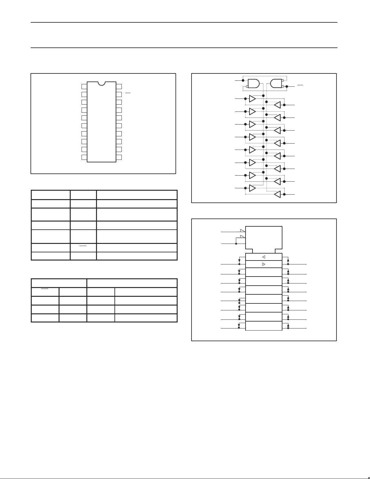
PIN CONFIGURATION
1
DIR
2
A0
3
A1
4
A2
5
A3
6
A4
7
A5
8
A6
9
A7
10 11
GND
PIN DESCRIPTION
PIN NUMBER SYMBOL FUNCTION
1 DIR Direction control
2, 3, 4, 5, 6,
7, 8, 9
A0 to A7Data inputs/outputs
10 GND Ground (0V)
18, 17, 16, 15,
14, 13, 12, 11
B0 to B7Data inputs/outputs
19 OE Output enable input (active-Low)
20 V
Positive supply voltage
CC
FUNCTION TABLE
INPUTS INPUTS/OUTPUTS
OE DIR
L L A = B Inputs
L H lnputs B = A
H X Z Z
H = HIGH voltage level
L = LOW voltage level
X = Don’t care
Z = High impedance OFF-state
An
20
19
18
17
16
15
14
13
12
SV00014
V
OE
B0
B1
B2
B3
B4
B5
B6
B7
CC
B
0
LOGIC SYMBOL
1
DIR
2
A0
3
A1
4
A2
5
A3
6
A4
7
A5
8
A6
9
A7
LOGIC SYMBOL (IEEE/IEC)
19
1
2
3
4
5
6
7
8
9
G3
3EN1 (BA)
3EN2 (AB)
∇ 1
74LVC245A
74LVCH245A
19
OE
18
B0
17
B1
16
B2
15
B3
14
B4
13
B5
12
B6
11
B7
SV00016
2 ∇
18
17
16
15
14
13
12
11
SV00208
1998 May 20
3
 Loading...