

Philips 74lvch2373a DATASHEETS
INTEGRATED CIRCUITS
74LVC2373A
74LVCH2373A
Octal D-type transparent latch with 5-volt
tolerant inputs/outputs; damping resistor
(3-State)
Product specification
IC24 Data Handbook
1997 Mar 12
Philips Semiconductors Product specification
Octal D-type transparent latch with 5-volt tolerant
inputs/outputs; damping resistor (3-State)
FEA TURES
•5-volt tolerant inputs/outputs, for interfacing with 5-volt logic
•Supply voltage range of 2.7V to 3.6V
•Complies with JEDEC standard no. 8-1A
•CMOS low power consumption
•Direct interface with TTL levels
•High impedance when V
CC
= 0V
•Bushold on all data inputs (74LVCH2373A only)
•Integrated 30 damping resistor
QUICK REFERENCE DATA
GND = 0V; T
SYMBOL
t
PHL/tPLH
C
I
C
PD
NOTES:
is used to determine the dynamic power dissipation (PD in µW)
1. C
PD
= CPD × V
P
D
= input frequency in MHz; CL = output load capacity in pF;
f
i
= output frequency in MHz; VCC = supply voltage in V;
f
o
Σ (C
L
2. The condition is V
= 25°C; tr = tf 2.5 ns
amb
Propagation delay
Dn to Qn
LE to Qn
Input capacitance 5.0 pF
Power dissipation capacitance per latch Notes 1, 2 20 pF
2
× fi Σ (CL × V
CC
2
× V
× fo) = sum of the outputs.
CC
= GND to V
I
PARAMETER CONDITIONS TYPICAL UNIT
2
× fo) where:
CC
CC.
DESCRIPTION
The 74LVC2373A/74LVCH2373A is a high performance, low-power,
low-voltage Si-gate CMOS device and superior to most advanced
CMOS compatible TTL families. Inputs can be driven from either
3.3V or 5V devices. This feature allows the use of these devices as
translators in a mixed 3.3V/5V environment.
The 74LVC2373A/74LVCH2373A is an octal D-type transparent
latch featuring separate D-type inputs for each latch and 3-State
outputs for bus oriented applications. A latch enable (LE) input and
an output enable (OE
The ‘2373’ consists of eight D-type transparent latches with 3-State
true outputs. When LE is HIGH, data at the Dn inputs enters the
latches. In this condition the latches are transparent, i.e., a latch
output will change each time its corresponding D-input changes.
When LE is LOW the latches store the information that was present
at the D-inputs a set-up time preceding the HIGH-to-LOW transition
of LE. When OE
available at the outputs. When OE
high impedance OFF-state. Operation of the OE
affect the state of the latches.
CL = 50pF
= 3.3V 4.4
V
CC
74L VC2373A
74L VCH2373A
) input are common to all internal latches.
is LOW, the contents of the eight latches are
is HIGH, the outputs go to the
input does not
ns
5.0
ORDERING AND PACKAGE INFORMA TION
PACKAGES TEMPERATURE RANGE
20-Pin Plastic SO –40°C to +85°C 74LVC2373A D 74LVC2373A D SOT163-1
20-Pin Plastic SSOP Type II –40°C to +85°C 74LVC2373A DB 74LVC2373A DB SOT339-1
20-Pin Plastic TSSOP Type I –40°C to +85°C 74LVC2373A PW LVC2373APW DH SOT360-1
20-Pin Plastic SO –40°C to +85°C 74LVCH2373A D 74LVCH2373A D SOT163-1
20-Pin Plastic SSOP Type II –40°C to +85°C 74LVCH2373A DB 7LVCH2373A DB SOT339-1
20-Pin Plastic TSSOP Type I –40°C to +85°C 74LVCH2373A PW VCH2373APW DH SOT360-1
1997 Mar 12 853–1940 17843
OUTSIDE NORTH
AMERICA
2
NORTH AMERICA PKG. DWG. #
Philips Semiconductors Product specification
Octal D-type transparent latch with 5-volt tolerant
inputs/outputs; damping resistor (3-State)
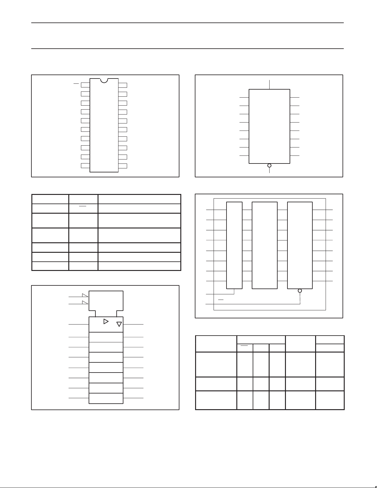
PIN CONFIGURATION
OE
GND
Q0
D0
D1
Q1
Q2
D2
D3
Q3
1
2
3
4
5
6
7
8
9
10
20
V
CC
19
Q7
18
D7
17
D6
16
Q6
15
Q5
14
D5
13
D4
Q4
12
11
LE
PIN DESCRIPTION
PIN NUMBER SYMBOL FUNCTION
1 OE Output enable input (active LOW)
2, 5, 6, 9, 12,
15, 16, 19
3, 4, 7, 8, 13,
14, 17, 18
Q0–Q7 3-State latch outputs
D0–D7 Data inputs
10 GND Ground (0V)
11 LE Latch enable input (active HIGH)
20 V
Positive supply voltage
CC
LOGIC SYMBOL (IEEE/IEC)
11
C1
1
EN1
SV00657
LOGIC SYMBOL
FUNCTIONAL DIAGRAM
74LVC2373A
74LVCH2373A
11
D0
D1
D2
D3
D4
D5
D6
D7
OE
LATCH
1 to 8
LE
1
Q0
Q1
Q2
Q3
Q4
Q5
Q6
Q7
2
5
6
9
12
15
16
19
3–STATE
OUTPUTS
Q0
Q1
Q2
Q3
Q4
Q5
Q6
Q7
SV00658
2
5
6
9
12
15
16
19
3
4
7
8
13
14
17
18
3
D0
4
D1
7
D2
8
D3
13
D4
14
D5
17
D6
18
D7
11
LE
1
OE
1997 Mar 12
3
1D
4
7
8
13
14
17
18
2
5
6
9
12
15
16
19
SV00659
FUNCTION TABLE
OPERATING
MODES
Enable and
read register
(transparent
mode)
Latch and read
register
Latch register
and disable
outputs
OE LE Dn
L
L
L
L
H
H
INPUTS
H
H
L
L
L
L
L
H
I
h
I
h
INTERNAL
LATCHES
L
H
L
H
L
H
SV00660
OUTPUTS
Q0 to Q7
L
H
L
H
Z
Z
H = HIGH voltage level
h = HIGH voltage level one set-up time prior to the HIGH-to-LOW
LE transition
L = LOW voltage level
I = LOW voltage level one set-up time prior to the HIGH-to-LOW
LE transition
X = Don’t care
Z = High impedance OFF-state
3
Philips Semiconductors Product specification
SYMBOL
PARAMETER
CONDITIONS
UNIT
mW
Octal D-type transparent latch with 5-volt tolerant
inputs/outputs; damping resistor (3-State)
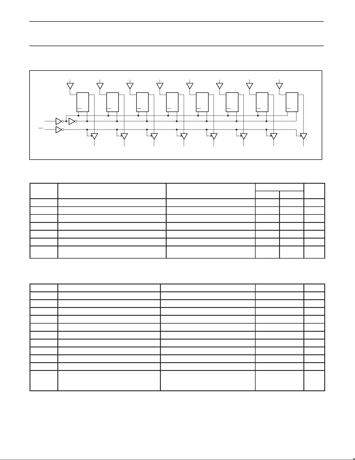
LOGIC DIAGRAM
D0
D
LATCH
1
LE
LE
OE
RECOMMENDED OPERATING CONDITIONS
V
V
T
V
V
V
amb
tr, t
DC supply voltage (for max. speed performance) 2.7 3.6 V
CC
DC supply voltage (for low-voltage applications) 1.2 3.6 V
CC
DC input voltage range 0 5.5 V
I
DC input voltage range for I/Os 0 V
I/O
DC output voltage range 0 V
O
Operating free-air temperature range –40 +85 °C
Input rise and fall times
f
D1
Q
LE
Q0
D
LATCH
2
LE
D2
Q
LE
Q1
D
LATCH
3
LE
D3
Q
LE
Q2
D
LATCH
4
LE
D4
Q
LE
Q3
VCC = 1.2 to 2.7V
V
CC
Q
D
LATCH
5
LE
LE
Q4
= 2.7 to 3.6V
74LVC2373A
74LVCH2373A
D5
D
LATCH
6
LE
D6
Q
LE
Q5
D
LATCH
7
LE
D7
Q
LE
Q6
D
LATCH
8
LE
Q
LE
Q7
SV00661
LIMITS
MIN MAX
CC
CC
0
0
20
10
V
V
ns/V
ABSOLUTE MAXIMUM RATINGS
1
In accordance with the Absolute Maximum Rating System (IEC 134).
Voltages are referenced to GND (ground = 0V).
SYMBOL
V
CC
I
IK
V
I
V
I/O
I
OK
V
OUT
V
OUT
I
OUT
I
, I
GND
CC
T
stg
DC supply voltage –0.5 to +6.5 V
DC input diode current VI t0 –50 mA
DC input voltage Note 2 –0.5 to +5.5 V
DC input voltage range for I/Os –0.5 to VCC +0.5 V
DC output diode current V
DC output voltage; output HIGH or LOW Note 2 –0.5 to VCC +0.5 V
DC output voltage; output 3-State Note 2 –0.5 to +6.5 V
DC output source or sink current VO = 0 to V
DC VCC or GND current ±100 mA
Storage temperature range –60 to +150 °C
PARAMETER CONDITIONS RATING UNIT
uVCC or VO t 0 ±50 mA
O
CC
±50 mA
Power dissipation per package
P
TOT
– plastic mini-pack (SO) above +70°C derate linearly with 8 mW/K 500
– plastic shrink mini-pack (SSOP and TSSOP) above +60°C derate linearly with 5.5 mW/K 500
NOTES:
1. Stresses beyond those listed may cause permanent damage to the device. These are stress ratings only and functional operation of the
device at these or any other conditions beyond those indicated under “recommended operating conditions” is not implied. Exposure to
absolute-maximum-rated conditions for extended periods may affect device reliability .
2. The input and output voltage ratings may be exceeded if the input and output current ratings are observed.
1997 Mar 12
4
 Loading...