

Philips 74LVCH16541ADL, 74LVCH16541ADGG Datasheet

74LVCH16541A
16-bit buffer/line driver (3-State)
Product specification
IC24 Data Handbook
1998 May 19
INTEGRATED CIRCUITS
Philips Semiconductors Product specification
74L VCH16541A16-bit buffer/line driver; 5V tolerant I/O (3-State)
2
1998 May 19 853-2063 19403
FEA TURES
•5 volt tolerant inputs/outputs for interfacing with 5V logic
•Wide supply voltage range of 1.2 V to 3.6 V
•Drive capability ±24mA @ 3.3V
•Complies with JEDEC standard no. 8-1A
•CMOS low power consumption
•MULTIBYTE
TM
flow-through standard pin-out architecture
•Low inductance multiple power and ground pins for minimum
noise and ground bounce
•Direct interface with TTL levels
•All data inputs have bushold
•Bushold inputs eliminate the need for external pull-up resistors to
hold unused inputs
DESCRIPTION
The 74LVCH16541A is a high-performance, low-power, low-voltage,
Si-gate CMOS device, superior to most advanced CMOS
compatible TTL families. Inputs can be driven from either 3.3V or 5V
devices. In 3-State operation, outputs can handle 5V . These
features allow the use of these devices in a mixed 3.3V/5V
environment.
The 74LVCH16541A is a 16-bit inverting buf fer/line driver with
3-State outputs. The 3-State outputs are controlled by the output
enable inputs 1OE
n
and 2OEn. A HIGH on nOEn causes the outputs
to assume a high impedance OFF-state.
To ensure the high impedance state during power up or power
down, OE
should be tied to VCC through a pullup resistor; the
minimum value of the resistor is determined by the current-sinking
capability of the driver.
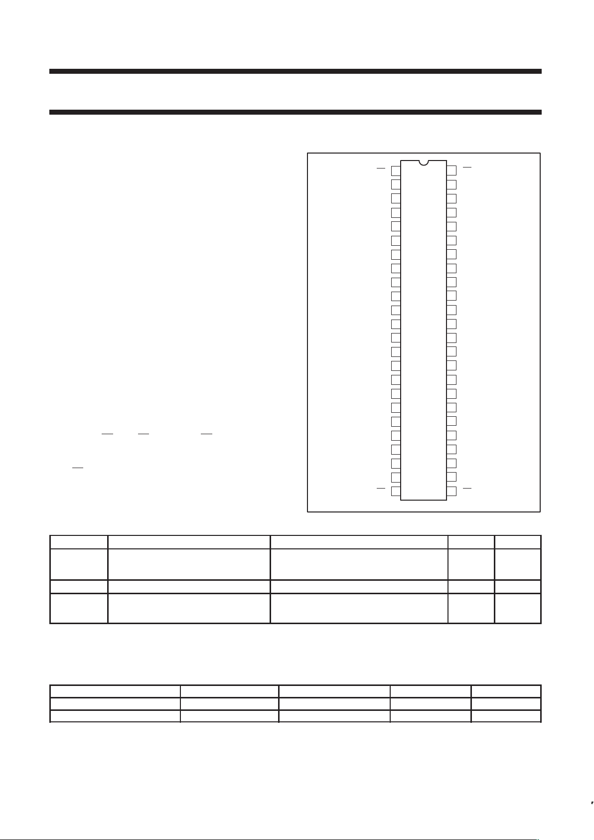
PIN CONFIGURATION
1
2
3
4
5
6
7
8
9
10
11
12
13
14
15
16
17
18
19
20
29
30
31
32
33
34
35
36
37
38
39
40
41
42
43
44
45
46
47
48
1OE
1
1Y0
1Y1
GND
1Y2
1Y3
V
CC
1Y5
GND
1Y6
1Y7
2Y0
2Y1
GND
1Y4
2Y2
2Y3
V
CC
2Y4
2Y5
2A5
2A4
V
CC
2A3
2A2
GND
2A1
2A0
1A7
1A6
GND
1A5
1A4
V
CC
1A3
1A2
GND
1A1
1A0
1OE
2
21
22
23
24
25
26
27
28
GND
2Y6
2Y7
2OE
1
2OE
2
2A7
2A6
GND
SW00113
QUICK REFERENCE DA TA
GND = 0V; T
amb
= 25°C; tr = tf ≤ 2.5ns
SYMBOL
PARAMETER CONDITIONS TYPICAL UNIT
t
PHL/tPLH
Propagation delay
1An to 1Yn;
2An to 2Yn
CL = 50pF
VCC = 3.3V
2.7 ns
C
I
Input capacitance 5.0 pF
C
PD
Power dissipation capacitance per buffer
VI = GND to V
CC
1
outputs enabled
output disabled
32
5
pF
NOTES:
1. C
PD
is used to determine the dynamic power dissipation (PD in W): PD = CPD × V
CC
2
× fi + (CL × V
CC
2
× fo) where:
f
i
= input frequency in MHz; CL = output load capacitance in pF; fo = output frequency in MHz; VCC = supply voltage in V;
(C
L
× V
CC
2
× fo) = sum of outputs.
ORDERING INFORMATION
PACKAGES TEMPERATURE RANGE OUTSIDE NORTH AMERICA NORTH AMERICA DWG NUMBER
48-Pin Plastic SSOP Type III –40°C to +85°C 74LVCH16541A DL VCH16541A DL SOT370-1
48-Pin Plastic TSSOP Type II –40°C to +85°C 74LVCH16541A DGG VCH16541A DGG SOT362-1
Philips Semiconductors Product specification
74LVCH16541A
16-bit buffer/line driver; 5V tolerant I/O (3-State)
1998 May 19
3
PIN DESCRIPTION
PIN NUMBER SYMBOL NAME AND FUNCTION
1, 24 nOE
1
Output enable input
(active LOW)
2, 3, 5, 6, 8, 9,
11, 12
1Y0 to 1Y7 Data outputs
4, 10, 15, 21,
28, 34, 39, 45
GND Ground (0V)
7, 18, 31, 42 V
CC
Positive supply voltage
13, 14, 16, 17,
19, 20, 22, 23
2Y0 to 2Y7 Data outputs
25, 48 nOE
2
Output enable input
(active LOW)
36, 35, 33, 32,
30, 29, 27, 26
2A0 to 2A7 Data inputs
47, 46, 44, 43,
41, 40, 38, 37
1A0 to 1A7 Data inputs
LOGIC SYMBOL
1A0
47 2
1Y0
1A1
46 3
1Y1
1A2
44 5
1Y2
1A3
43 6
1Y3
1A4
41 8
1Y4
1A5
40 9
1Y5
1A6
38 11
1Y6
1A7
37 12
1Y7
1OE
1
1
1OE
2
48
2A0
36 13
2Y0
2A1
35 14
2Y1
2A2
33 16
2Y2
2A3
32 17
2Y3
2A4
30 19
2Y4
2A5
29 20
2Y5
2A6
27 22
2Y6
2A7
26 23
2Y7
2OE
1
24
2OE
2
25
SW00115
FUNCTION T ABLE
INPUTS OUTPUT
nOE
1
nOE
2
nAn nYn
L L L L
L L H H
X H X Z
H X X Z
H = HIGH voltage level
L = LOW voltage level
X = don’t care
Z = high impedance OFF-state
LOGIC SYMBOL (IEEE/IEC)
48
1 ∇
46
44
43
41
40
38
37
36
EN
1
2 ∇2
1
25
24
47
35
33
32
30
29
27
26
3
2
5
6
8
9
11
12
13
14
16
17
19
20
22
23
SW00114
1OE
1
1OE
2
2OE
1
2OE
2
1A0
1A1
1A2
1A3
1A4
1A5
1A6
2A0
2A1
2A2
2A3
2A4
2A5
2A6
2A7
1Y0
1Y1
1Y2
1Y3
1Y4
1Y5
1Y6
1Y7
2Y0
2Y1
2Y2
2Y3
2Y4
2Y7
1A7
2Y5
2Y6
&
&
BUSHOLD CIRCUIT
To internal circuit
V
CC
Data Input
SW00044
 Loading...