

Philips 74LVCH16245ADL, 74LVCH16245ADGG, 74LVC16245ADL, 74LVC16245ADGG Datasheet

INTEGRATED CIRCUITS
74LVC16245A/
74LVCH16245A
16-bit bus transceiver with direction pin;
5V tolerant (3-State)
Product specification
Supersedes data of 1997 Aug 1
IC24 Data Handbook
1997 Sep 25
Philips Semiconductors Product specification
16-bit bus transceiver with direction pin; 5V tolerant
(3-State)
FEA TURES
•5 volt tolerant inputs/outputs for interfacing with 5V logic
•Wide supply voltage range of 1.2V to 3.6V
•Complies with JEDEC standard no. 8-1A
•CMOS low power consumption
•MULTIBYTE
TM
flow-through standard pin-out architecture
•Low inductance multiple power and ground pins for minimum
noise and ground bounce
•Direct interface with TTL levels
•High impedance when V
CC
= 0
•All data inputs have bus hold (74LVCH16245A only)
DESCRIPTION
The 74LVC(H)16245A is a high-performance, low-power,
low-voltage, Si-gate CMOS device, superior to most advanced
CMOS compatible TTL families. Inputs can be driven from either
3.3V or 5V devices. In 3-State operation, outputs can handle 5V .
These features allow the use of these devices in a mixed 3.3V/5V
environment.
The 74LVC(H)16245A is a 16-bit transceiver featuring non-inverting
3-State bus compatible outputs in both send and receive directions.
The 74LVC(H)16245A features two output enable (nOE
easy cascading and two send/receive (nDIR) inputs for direction
control. nOE
controls the outputs so that the buses are effectively
isolated. This device can be used as two 8-bit transceivers or one
16-bit transceiver.
The 74LVCH16245A bus hold data inputs eliminates the need for
extreme pull up resistors to hold unused inputs.
) inputs for
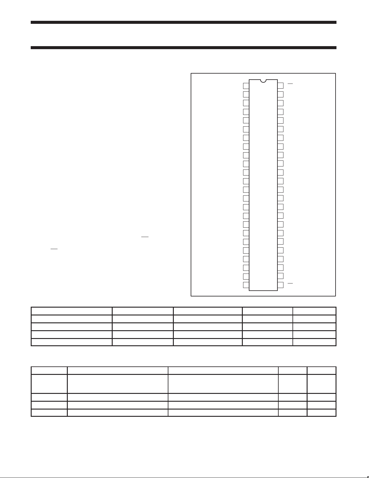
PIN CONFIGURATION
1DIR
1B0
1B1
GND
1B2
1B3
V
CC1
1B4
1B5
GND
1B6
1B7
2B0
2B1
GND
2B2
2B3
V
CC1
2B4
2B5
GND
2B6
2B7
2DIR
74L VC16245A/
74L VCH16245A
1OE
SW00198
48
47
1A0
46
1A1
45
GND
44
1A2
43
1A3
42
V
CC2
41
1A4
40
1A5
39
GND
38
1A6
37
1A7
36
2A0
35
2A1
34
GND
33
2A2
32
2A3
31
V
CC2
30
2A4
29
2A5
28
GND
27
2A6
26
2A7
25
2OE
1
2
3
4
5
6
7
8
9
10
11
12
13
14
15
16
17
18
19
20
21
22
23
24
ORDERING INFORMA TION
PACKAGES TEMPERATURE RANGE OUTSIDE NORTH AMERICA NORTH AMERICA DWG NUMBER
48-Pin Plastic SSOP Type III –40°C to +85°C 74LVC16245A DL VC16245A DL SOT370-1
48-Pin Plastic TSSOP Type II –40°C to +85°C 74LVC16245A DGG VC16245A DGG SOT362-1
48-Pin Plastic SSOP Type III –40°C to +85°C 74LVCH16245A DL VCH16245A DL SOT370-1
48-Pin Plastic TSSOP Type II –40°C to +85°C 74LVCH16245A DGG VCH16245A DGG SOT362-1
QUICK REFERENCE DATA
GND = 0V; T
SYMBOL
t
PHL/tPLH
C
I
C
I/O
C
PD
NOTES:
1. C
is used to determine the dynamic power dissipation (PD in µW):
PD
= CPD × V
P
D
f
= input frequency in MHz; CL = output load capacity in pF;
i
= output frequency in MHz; VCC = supply voltage in V;
f
o
(C
1997 Sep 25 853-2013 18424
= 25°C; tr = tf ≤ 2.5ns
amb
Propagation delay
An to Bn;
Bn to An
Input capacitance 5.0 pF
Input/output capacitance 10 pF
Power dissipation capacitance per buffer VI = GND to V
CC
2
× V
L
× fo) = sum of the outputs.
CC
2
× fi + (CL × V
PARAMETER CONDITIONS TYPICAL UNIT
2
× fo) where:
CC
CL = 50pF
VCC = 3.3V
CC
1
3.0 ns
30 pF
2
Philips Semiconductors Product specification
16-bit bus transceiver with direction pin; 5V tolerant
(3-State)
PIN DESCRIPTION
PIN NUMBER SYMBOL NAME AND FUNCTION
1 1DIR Direction control
2, 3, 5, 6, 8, 9,
11, 12
4, 10, 15, 21,
28, 34, 39, 45
7, 18, 31, 42 V
13, 14, 16, 17,
19, 20, 22, 23
1B0 to 1B7 Data inputs/outputs
GND Ground (0V)
CC
Positive supply voltage
2B0 to 2B7 Data inputs/outputs
24 2DIR Direction control
25 2OE
36, 35, 33, 32,
30, 29, 27, 26
47, 46, 44, 43,
41, 40, 38, 37
48 1OE
2A0 to 2A7 Data inputs/outputs
1A0 to 1A7 Data inputs/outputs
Output enable input
(active LOW)
Output enable input
(active LOW)
LOGIC SYMBOL
1DIR
1A0
1A1
1A2
1A3
1A4
1A5
1A6
1
48
1OE
47
46
44
43
41
40
38
2
1B0
3
1B1
5
1B2
6
1B3
8
1B4
9
1B5
11
1B6
2DIR
2A0
2A1
2A2
2A3
2A4
2A5
2A6
24
36
35
33
32
30
29
27
25
2OE
13
2B0
14
2B1
16
2B2
17
2B3
19
2B4
20
2B5
22
2B6
LOGIC SYMBOL (IEEE/IEC)
1OE
1DIR
2OE
2DIR
BUS HOLD CIRCUIT
1A0
1A1
1A2
1A3
1A4
1A5
1A6
1A7
2A0
2A1
2A2
2A3
2A4
2A5
2A6
2A7
74LVC16245A/
74LVCH16245A
48
1
25
24
47
46
44
43
41
40
38
37
36
35
33
32
30
29
27
26
G3
3 EN1 [BA]
3 EN2 [AB]
G6
6 EN4 [BA]
6 EN5 [AB]
1
2
4
5
V
CC
2
1B0
3
1B1
5
1B2
6
1B3
8
1B4
9
1B5
11
1B6
12
1B7
13
2B0
14
2B1
16
2B2
17
2B3
19
2B4
20
2B5
22
2B6
23
2B7
SW00196
37 12
1A7
1B7
26 23
2A7
FUNCTION TABLE
INPUTS INPUTS/OUTPUT
nOE nDIR nAn nBn
L L A = B inputs
L H inputs B = A
H X Z Z
H = HIGH voltage level
L = LOW voltage level
X = don’t care
Z = high impedance OFF-state
1997 Sep 25
2B7
SW00197
Data Input
To internal circuit
SW00044
3
 Loading...