

Philips 74LVCH162374ADL, 74LVCH162374ADGG, 74LVC162374ADL, 74LVC162374ADGG Datasheet

INTEGRATED CIRCUITS
DATA SH EET
74LVC162374A; 74LVCH162374A
16-bit edge triggered D-type
flip-flopwith30 Ωseriestermination
resistors; 5 V input/output tolerant;
3-state
Product specification
File under Integrated Circuits, IC24
1999 Aug 05
Philips Semiconductors Product specification
16-bit edge triggered D-type flip-flop with 30 Ω series
termination resistors; 5 V input/output tolerant; 3-state
FEATURES
• ESD protection:
HBM EIA/JESD22-A114-A
exceeds 2000 V
MM EIA/JESD22-A115-A
exceeds 200 V
• 5 V tolerant input/output for
interfacing with 5 V logic
• Wide supply voltage range of
1.2 to 3.6 V
• Complies with JEDEC standard
no. 8-1A
• CMOS low power consumption
• MULTIBYTE flow-through
standard pin-out architecture
• Lowinductancemultiple powerand
ground pins forminimum noiseand
ground bounce
• Direct interface with TTL levels
• All data inputs have bus hold
(74LVCH162374A only)
• High impedance when VCC=0
• Power off disables outputs,
permitting live insertion.
DESCRIPTION
The 74LVC(H)162374A is a 16-bit edge triggered flip-flop featuring separate
D-typeinputs foreachflip-flop and3-stateoutputs forbusoriented applications.
The 74LVC162374A consists of 2 sections of eight edge-triggered flip-flops.
A clock (CP) input and an output enable (OE) are provided for each octal.
Inputs can be driven from either 3.3 or 5 V devices. In 3-state operation,
outputs can handle 5 V. These features allow the use of these devices in a
mixed 3.3 and 5 V environment.
The flip-flops will storethe stateof their individual D-inputs thatmeet theset-up
and hold time requirements on the LOW-to-HIGH CP transition.
When OE is LOW, the contents of the flip-flops are available at the outputs.
When OE is HIGH, the outputs go to the high-impedance OFF-state.
Operation of the OE input does not affect the state of the flip-flops.
The74LVCH162374A bushold datainputs eliminates theneed forexternal pull
up resistors to hold unused inputs.
The 74LVC(H)162374A is designed with 30 Ω series termination resistors in
both HIGH and LOW output stages to reduce line noise.
74LVC162374A;
74LVCH162374A
FUNCTION TABLE
See note 1.
OPERATION MODES
Load and read register
Latch register and disable outputs
Note
1. H = HIGH voltage level;
h = HIGH voltage level one set-up time prior to the HIGH-to-LOW LE transition;
L = LOW voltage level;
l = LOW voltage level one set-up time prior to the HIGH-to-LOW LE transition;
Z = high-impedance OFF-state;
↑ = LOW-to-HIGH CP transition.
nOE nCP nD
L ↑ lL L
L↑hH H
H ↑ lL Z
H↑hH Z
INPUTS
INTERNAL
n
FLIP-FLOPS
OUTPUTS
Q0to Q
7
1999 Aug 05 2

Philips Semiconductors Product specification
16-bit edge triggered D-type flip-flop with 30 Ω series
termination resistors; 5 V input/output tolerant; 3-state
74LVC162374A;
74LVCH162374A
QUICK REFERENCE DATA
GND = 0 V; T
=25°C; tr=tf≤2.5 ns.
amb
SYMBOL PARAMETER CONDITIONS TYPICAL UNIT
t
PHL/tPLH
f
max
C
I
C
PD
propagation delay CP to Q
n
maximum clock frequency 150 MHz
input capacitance 5.0 pF
power dissipation capacitance per
CL= 50 pF; VCC= 3.3 V 3.8 ns
VCC= 3.3 V; note 1 30 pF
flip-flop
Note
1. C
is used to determine the dynamic power dissipation (PDin µW).
PD
PD=CPD× V
2
× fi+ ∑ (CL× V
CC
2
× fo) where:
CC
fi= input frequency in MHz;
= output frequency in MHz;
f
o
∑ (CL× V
2
× fo) = sum of outputs;
CC
CL= output load capacitance in pF;
VCC= supply voltage in Volts.
ORDERING INFORMATION
PACKAGE
OUTSIDE NORTH
AMERICA
NORTH AMERICA
TEMPERATURE
RANGE
PINS PACKAGE MATERIAL CODE
74LVC162374ADL VC162374A DL −40 to +85 °C 48 SSOP plastic SOT370-1
74LVC162374ADGG VC162374A DGG 48 TSSOP plastic SOT362-1
74LVCH162374ADL VCH162374A DL 48 SSOP plastic SOT370-1
74LVCH162374ADGG VCH162374A DGG 48 TSSOP plastic SOT362-1
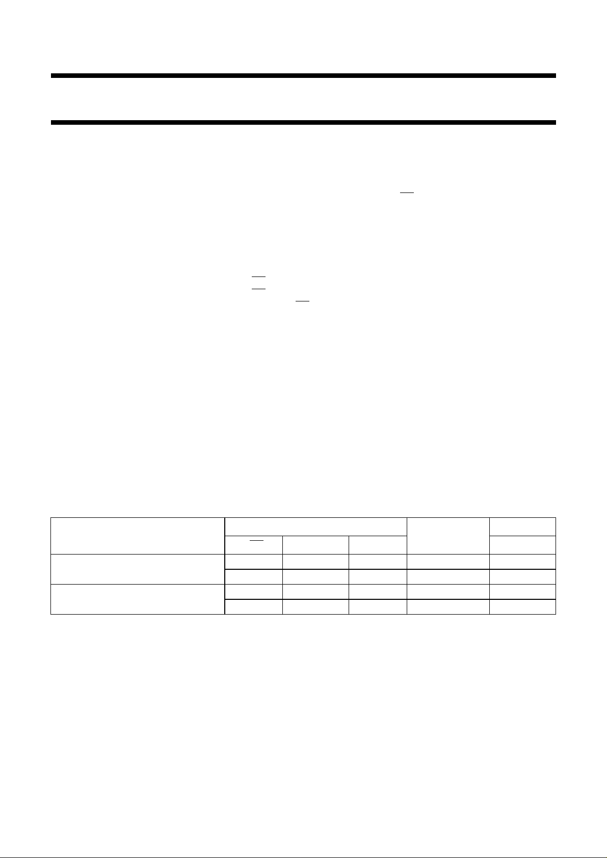
PINNING
PIN SYMBOL DESCRIPTION
11
2, 3, 5, 6, 8, 9, 11, 12 1Q
OE output enable input (active LOW)
to 1Q
0
7
3-state flip-flop outputs
4, 10, 15, 21, 28, 34, 39, 45 GND ground (0 V)
7, 18, 31, 42 V
13, 14, 16, 17, 19, 20, 22, 23 2Q
24 2
CC
to 2Q
0
7
OE output enable input (active LOW)
DC supply voltage
3-state flip-flop outputs
25 2CP clock input
36, 35, 33, 32, 30, 29, 27, 26 2D
47, 46, 44, 43, 41, 40, 38, 37 1D
to 2D
0
to 1D
0
7
7
data inputs
data inputs
48 1CP clock input
1999 Aug 05 3
Philips Semiconductors Product specification
16-bit edge triggered D-type flip-flop with 30 Ω series
termination resistors; 5 V input/output tolerant; 3-state
handbook, halfpage
1OE
1Q
1Q
GND
1Q
1Q
V
CC
1Q
1Q
GND
1Q
1Q
2Q
2Q
GND
2Q
2Q
V
CC
2Q
2Q
GND
2Q
2Q
2OE
1
2
0
3
1
4
5
2
6
3
7
8
4
9
5
10
11
6
12
7
162374A
13
0
14
1
15
16
2
17
3
18
19
4
20
5
21
22
6
23
7
24
MNA433
1CP
48
1D
47
0
1D
46
1
GND
45
1D
44
2
1D
43
3
V
42
CC
1D
41
4
1D
40
5
GND
39
1D
38
6
1D
37
7
2D
36
0
2D
35
1
GND
34
2D
33
2
2D
32
3
V
31
CC
2D
30
4
2D
29
5
GND
28
2D
27
6
2D
26
7
2CP
25
handbook, halfpage
47
46
44
43
41
40
38
37
36
35
33
32
30
29
27
26
74LVC162374A;
74LVCH162374A
1
24
1OE
2OE
1D
0
1D
1
1D
2
1D
3
1D
4
1D
5
1D
6
1D
7
2D
0
2D
1
2D
2
2D
3
2D
4
2D
5
2D
6
2D
7
1CP 2CP
48 25
1Q
1Q
1Q
1Q
1Q
1Q
1Q
1Q
2Q
2Q
2Q
2Q
2Q
2Q
2Q
2Q
0
1
2
3
4
5
6
7
0
1
2
3
4
5
6
7
MNA434
2
3
5
6
8
9
11
12
13
14
16
17
19
20
22
23
Fig.1 Pin configuration.
1999 Aug 05 4
Fig.2 Logic symbol.
Philips Semiconductors Product specification
16-bit edge triggered D-type flip-flop with 30 Ω series
termination resistors; 5 V input/output tolerant; 3-state
handbook, full pagewidth
1D
1CP
1OE
0
DCPQ
FF1
to 7 other channels
1Q
Fig.3 Logic diagram.
2D
0
0
2CP
2OE
DCPQ
to 7 other channels
FF2
74LVC162374A;
74LVCH162374A
2Q
0
MNA435
handbook, halfpage
1OE
1CP
2OE
2CP
1D
1D
1D
1D
1D
1D
1D
1D
2D
2D
2D
2D
2D
2D
2D
2D
1
1EN
48
C3
24
2EN
25
C2
47
46
44
43
41
40
38
37
36
35
33
32
30
29
27
26
1D 1
2D 2
MNA436
0
1
2
3
4
5
6
7
0
1
2
3
4
5
6
7
2
1Q
0
3
1Q
1
5
1Q
2
6
1Q
3
8
1Q
4
9
1Q
5
11
1Q
6
12
1Q
7
13
2Q
0
14
2Q
1
16
2Q
2
17
2Q
3
19
2Q
4
20
2Q
5
22
2Q
6
23
2Q
7
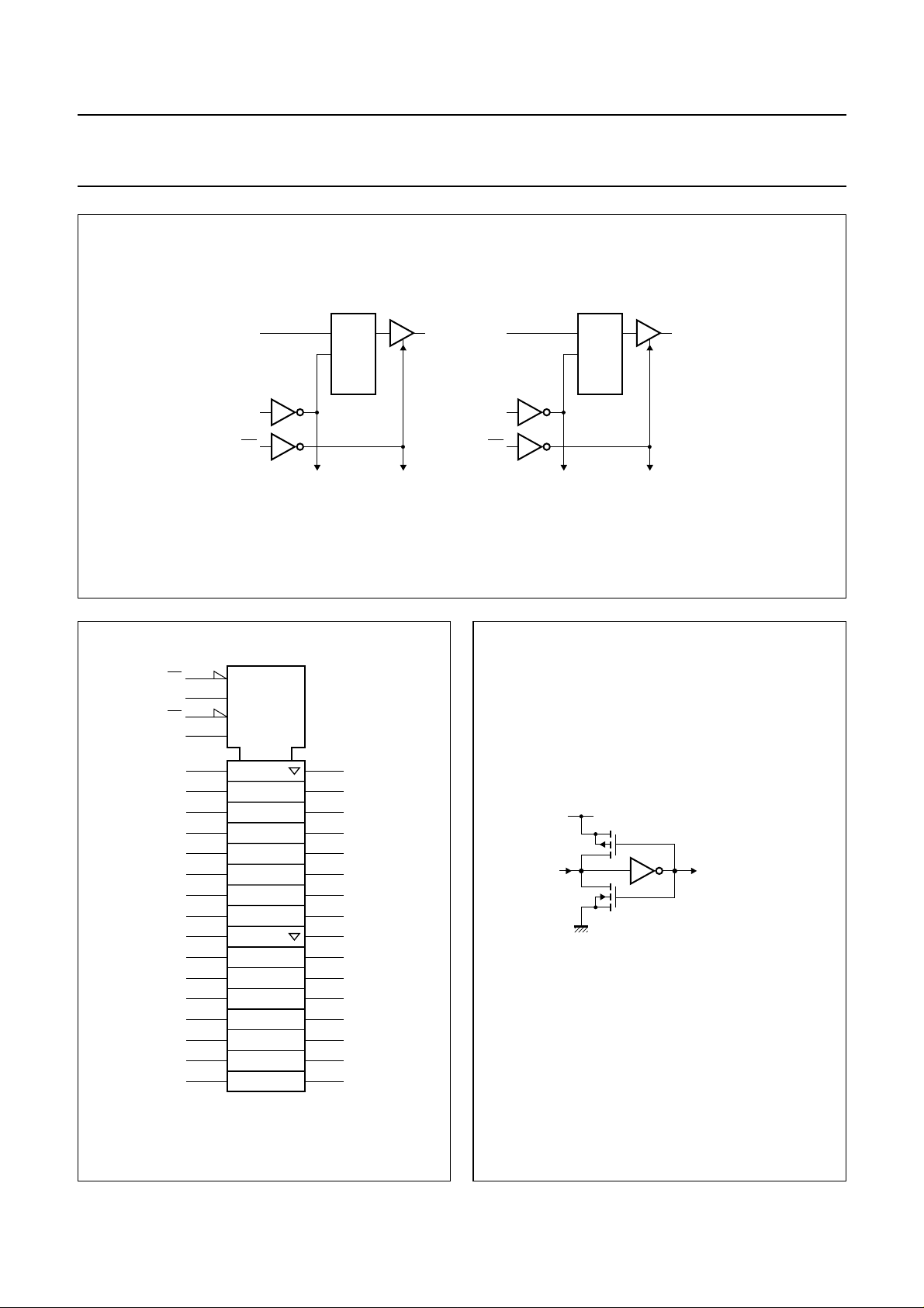
handbook, halfpage
input
V
CC
to internal circuit
MNA428
Fig.4 IEC logic symbol.
1999 Aug 05 5
Fig.5 Bus hold circuit.
 Loading...