

Philips 74lvc841a DATASHEETS
INTEGRATED CIRCUITS
74LVC841A
10-bit transparent latch with 5-volt
tolerant inputs/outputs (3-State)
Product specification
IC24 Data Handbook
1998 Jun 17
Philips Semiconductors Product specification
10-bit transparent latch with 5-volt tolerant
inputs/outputs (3-State)
FEA TURES
•5-volt tolerant inputs/outputs, for interfacing with 5-volt logic
•Wide supply voltage range of 1.2 V to 3.6 V
•In accordance with the JEDEC standard no. 8-1 A
•Inputs accept voltages up to 5.5 V
•CMOS low power consumption
•Direct interface with TTL levels
•Flow-through pin-out architecture
QUICK REFERENCE DATA
GND = 0 V; T
= 25°C; tr =t
amb
SYMBOL
Propagation delay
t
PHL/tPLH
C
I
C
PD
Dn to Qn;
LE to Q
Input capacitance 5.0 pF
Power dissipation capacitance per latch VI = GND to V
NOTE:
is used to determine the dynamic power dissipation (PD in µW)
1C
PD
P
= CPD × V
D
2
× fi (CL × V
CC
fi = input frequency in MHz; CL = output load capacity in pF;
f
= output frequency in MHz; VCC = supply voltage in V;
o
(C
2
× V
× fo) = sum o f t h e o u t p u t s .
L
CC
≤ 2.5 ns
f
PARAMETER CONDITIONS TYPICAL UNIT
CL = 50 pF;
VCC = 3.3 V
n
2
× fo) where:
CC
74L VC841A
DESCRIPTION
The 74LVC841A is a low-power, low-voltage, Si-gate CMOS device
and superior to most advanced CMOS compatible TTL families.
Inputs can be driven from either 3.3 V or 5 V devices. In 3-State
operation, outputs can handle 5 V . This feature allows the use of
these devices as translators in a mixed 3.3 V/5 V environment. The
74LVC841A is a 10-bit transparent latch featuring separate D-type
inputs for each latch and 3-State outputs for bus oriented
applications. A latch enable (LE) input and an output enable (OE
input are common to all internal latches. The 74LVC841A consists of
ten transparent latches with 3-State true outputs. When LE is HIGH,
data at the D
are transparent, i.e., a latch output will change each time its
inputs enters the latches. In this condition the latches
n
corresponding D-input changes. When LE is LOW the latches store
the information that was present at the D-inputs a set-up time
preceding the HIGH-to-LOW transition of LE. When OE is LOW, the
contents of the ten latches are available at the outputs.
When OE
Operation of the OE
is HIGH, the outputs go to the high impedance OFF-state.
input does not affect the state of the latches.
4.5
5.0
CC
1
22 pF
)
ns
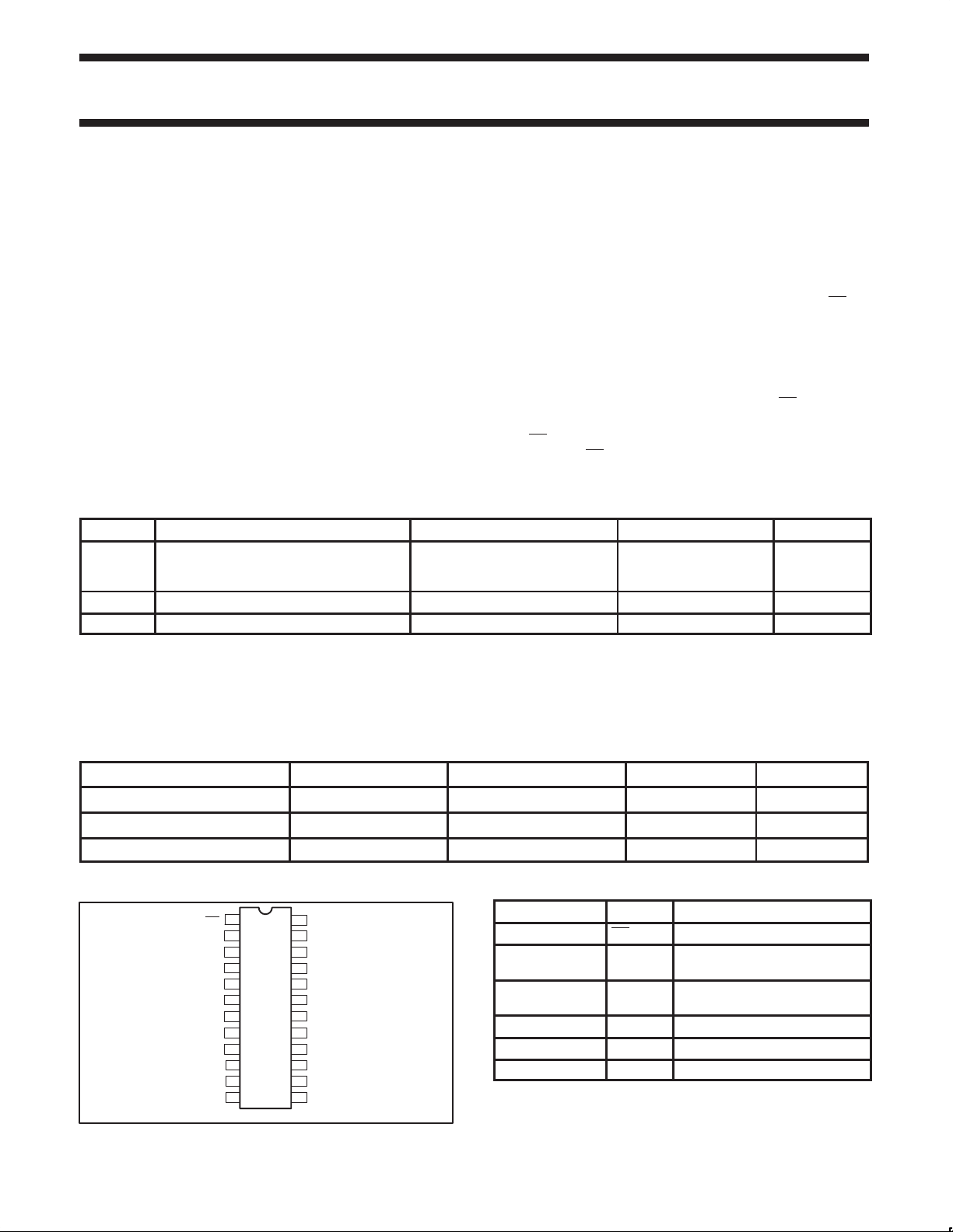
ORDERING INFORMATION
PACKAGES TEMPERATURE RANGE OUTSIDE NORTH AMERICA NORTH AMERICA PKG. DWG. #
24-Pin Plastic SO –40°C to +125°C 74LVC841A D 74LVC841A D SOT137-1
24-Pin Plastic SSOP Type II –40°C to +125°C 74LVC841A DB 74LVC841A DB SOT340-1
24-Pin Plastic TSSOP Type I –40°C to +125°C 74LVC841A PW 7LVC841APW DH SOT355-1
PIN CONFIGURATION
1
OE
2
D
0
3
D
1
4
D
2
5
D
3
6
D
4
7
D
5
8
D
6
9
D
7
10
D
8
11
D
9
12
GND
1998 Jun 17 853-2071 19589
24
23
22
21
20
19
18
17
16
15
14
13
SV01723
V
CC
Q
0
Q
1
Q
2
Q
3
Q
4
Q
5
Q
6
Q
7
Q
8
Q
9
LE
PIN DESCRIPTION
PIN NUMBER SYMBOL NAME AND FUNCTION
1 OE Output enable input (active Low)
2, 3, 4, 5, 6, 7, 8,
9, 10, 11
23, 22, 21, 20, 19,
18, 17, 16, 15, 14
12 GND Ground (0 V)
13 LE Latch enable input (active HIGH)
24 V
2
D0 to D9Data inputs
Q0 to Q93-state latch outputs
CC
Positive supply voltage
Philips Semiconductors Product specification
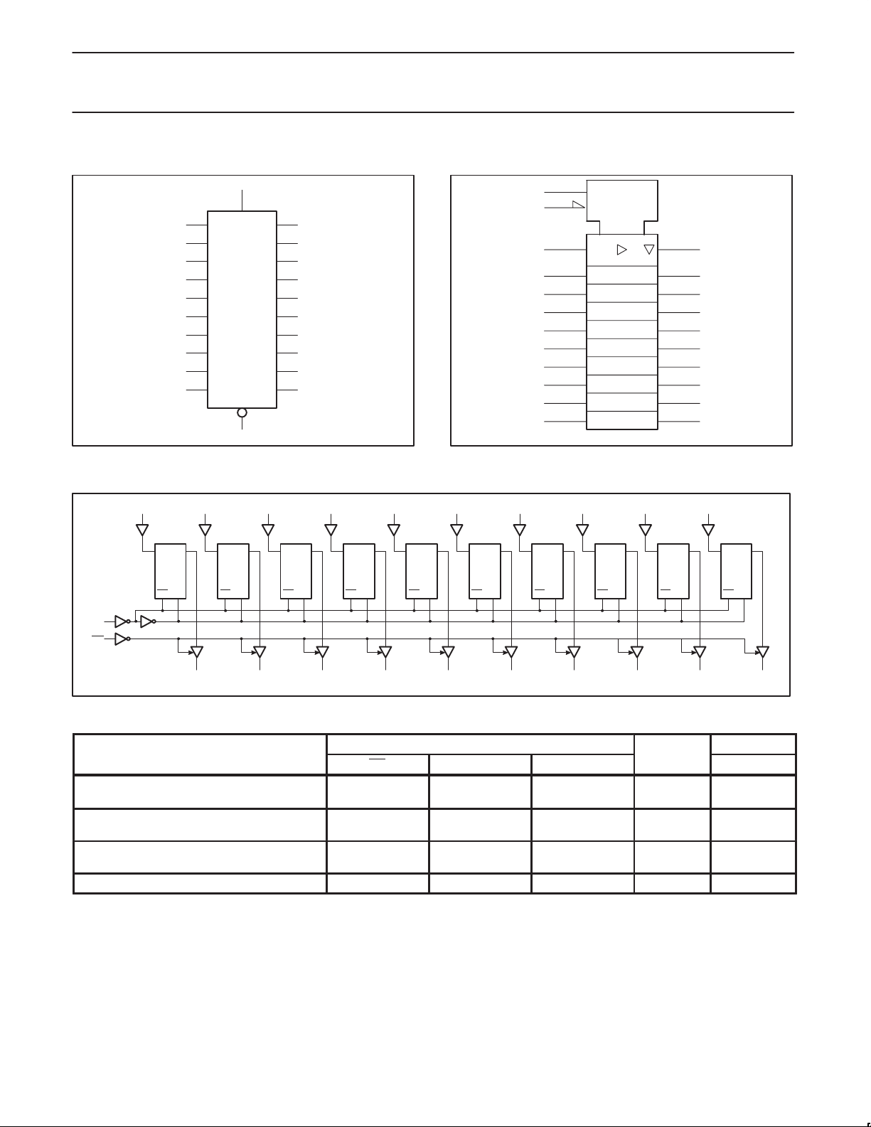
OPERATING MODES
10-bit transparent latch with 5-volt tolerant
inputs/outputs (3-State)
LOGIC SYMBOL (IEEE/IEC)
13
2
3
4
5
6
7
8
9
10
11
LOGIC DIAGRAM
LE
D
D
D
D
D
D
D
D
D
D
Q
0
Q
1
Q
2
Q
3
Q
4
Q
5
Q
6
Q
7
Q
8
Q
9
OE
1
0
1
2
3
4
5
6
7
8
9
SV01724
23
22
21
20
19
18
17
16
15
14
LOGIC SYMBOL
13
1
2
3
4
5
6
7
8
9
10
11
C1
EN
1D
74LVC841A
23
22
21
20
19
18
17
16
15
14
SV01725
D
0
DQ
LATCH
LE LE
LE
OE
FUNCTION TABLE for register An or B
Enable and read register (transparent mode)
Latch and read register
latch register and disable outputs
D
1
DQ
1
LATCH
LE LE
Q
0
D
2
DQ
2
LATCH
LE LE
Q
1
D
3
DQ
3
LATCH
LE LE
Q
2
D
4
DQ
4
LATCH
LE LE
Q
3
D
5
DQ
5
LATCH
LE LE
Q
4
D
6
DQ
6
LATCH
LE LE
Q
5
DD
7
DDD
7
LATCH
LE LELE LE LELE LE LE
QQ
6
D
8
QQQ
8
LATCH
LE
Q
7
D
9
9
LATCH
10
Q
8
SV01726
n
INPUTS
OE LE D
L
L
L
L
H
H
H
H
↓
↓
X
X
INTERNAL
n
L
H
l
h
l
h
LATCHES
L
H
L
H
L
H
OUTPUTS
Q0 TO Q
Hold L L X NC NC
NOTES:
H = HIGH voltage level
h = HIGH voltage level one set-up time prior to the HIGH-to-LOW LE transition
L = LOW voltage level
l = LOW voltage level one set-up time prior to the HIGH-to-LOW LE transition
X = don’t care
Z = high impedance OFF-state
NC = no change
Q
9
9
L
H
L
H
Z
Z
1998 Jun 17
3
 Loading...