

Philips 74lvc827a DATASHEETS
INTEGRATED CIRCUITS
74LVC827A
10-bit buffer/line driver with 5-volt tolerant
inputs/outputs (3-State)
Poduct specification 1998 Sep 04
Philips Semiconductors Product specification
10-bit buffer/line driver with 5-volt tolerant
inputs/outputs (3-State)
FEA TURES
•5-volt tolerant inputs/outputs, for interfacing with 5-volt logic
•Supply voltage range of 2.7V to 3.6V
•Complies with JEDEC standard no. 8-1A
•CMOS low power consumption
•Direct interface with TTL levels
•High impedance when V
QUICK REFERENCE DATA
GND = 0 V; T
SYMBOL
t
NOTES:
is used to determine the dynamic power dissipation (PD in µW)
1. C
PD
P
= CPD × V
D
fi = input frequency in MHz; CL = output load capacity in pF;
= output frequency in MHz; VCC = supply voltage in V;
f
o
(C
L
2. The condition is VI = GND to V
= 25°C; tr = tf ≤ 2.5 ns
amb
PHL/tPLH
C
I
C
PD
2
× fi (CL × V
CC
2
× V
× fo) = sum of the outputs.
CC
= 0V
CC
PARAMETER CONDITIONS TYPICAL UNIT
Propagation delay
An to Y
n
Input capacitance 5.0 pF
Power dissipation capacitance per buffer Notes 1 and 2 24 pF
2
× fo) where:
CC
CC
DESCRIPTION
The 74LVC827A is a high performance, low-power, low-voltage
Si-gate CMOS device and superior to most advanced CMOS
compatible TTL families.
Inputs can be driven from either 3.3V or 5.0V devices. In 3-state
operation, outputs can handle 5V. This feature allows the use of
these devices as translators in a mixed 3.3V/5V environment.
The 74LVC827A is a10-bit buf fer/line driver with 3-State outputs The
3-State outputs are controlled by the output enable inputs OE
OE
A HIGH on OE
OFF-state.
CL = 50 pF;
VCC = 3.3 V
74L VC827A
and
.
2
causes the outputs to assume a high impedance
n
4 ns
1
ORDERING INFORMATION
PACKAGES TEMPERATURE RANGE OUTSIDE NORTH AMERICA NORTH AMERICA PKG. DWG. #
24-Pin Plastic SO –40°C to +85°C 74LVC827A D 74LVC827A D SOT137-1
24-Pin Plastic SSOP Type II –40°C to +85°C 74LVC827A DB 74LVC827A DB SOT340-1
24-Pin Plastic TSSOP Type I –40°C to +85°C 74LVC827A PW 7LVC827APW DH SOT355-1
PIN DESCRIPTION
PIN NUMBER SYMBOL NAME AND FUNCTION
1, 13 OE1, OE
2, 3, 4, 5, 6,
7, 8, 9, 10, 11
12 GND Ground (0 V)
23, 22, 21, 20,
19, 18, 17, 16,
15, 14
24 V
A0 to A9Data inputs
Y0 to Y9Bus outputs
CC
Output enable input
2
(active LOW)
Positive supply voltage
FUNCTION TABLE
INPUTS OUTPUTS
OE
1
L L L L
L L H H
X H X Z
H X X Z
H = HIGH voltage level
L = LOW voltage level
X = Don’t care
Z = high impedance OFF-state
OE
2
An Yn
1998 Sep 04 853–21 17 19969
2
Philips Semiconductors Product specification
10-bit buffer/line driver with 5-volt tolerant
inputs/outputs (3-State)
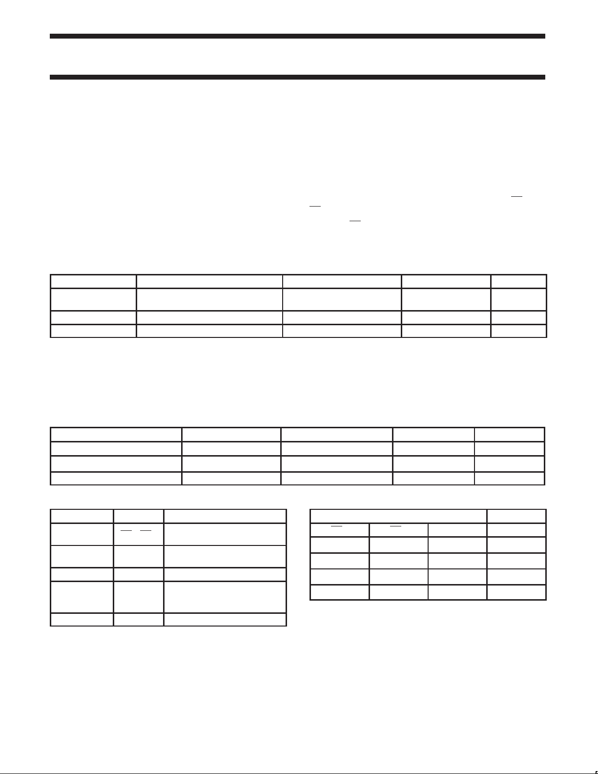
PIN CONFIGURATION
OE
GND
1
1
A
2
0
3
A
1
4
A
2
A
5
3
A
6
4
A
7
5
8
A
6
9
A
7
10
A
8
11
A
9
12
24
V
CC
23
Y
0
22
Y
1
Y
21
2
Y
20
3
Y
19
4
18
Y
5
17
Y
6
Y
16
7
Y
15
8
Y
14
9
13
OE
2
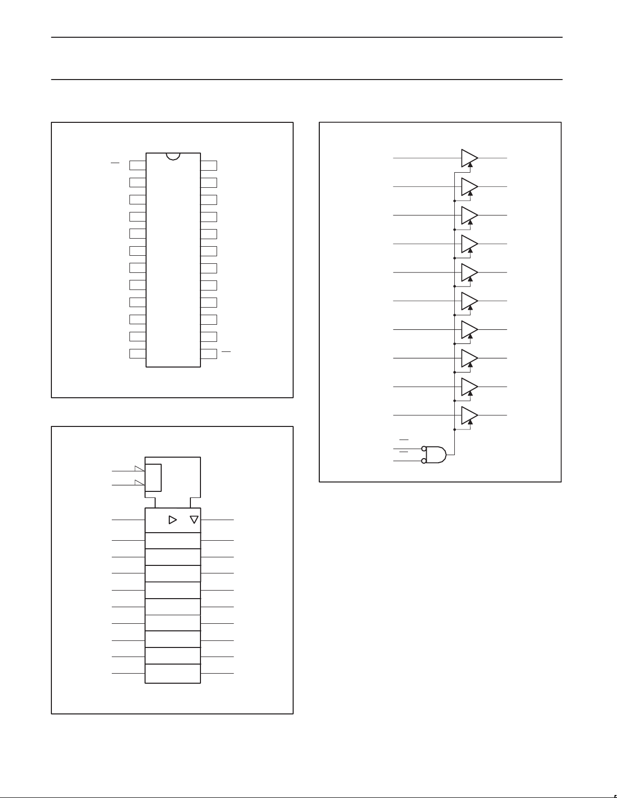
LOGIC SYMBOL
2
3
4
5
6
7
8
9
74LVC827A
A
0
A
1
A
2
A
3
A
4
A
5
A
6
A
7
Y
0
23
Y
1
22
Y
2
21
Y
3
20
Y
4
19
Y
5
18
Y
6
17
Y
7
16
LOGIC SYMBOL (IEEE/IEC)
1
&
13
2
3
4
5
6
7
8
9
10
11
EN
SA00426
A
OE
OE
8
A
9
1
2
10
11
1
13
23
22
21
20
19
18
17
16
15
14
Y
8
Y
9
SA00427
15
14
1998 Sep 04
SA00428
3
Philips Semiconductors Product specification
SYMBOL
PARAMETER
CONDITIONS
UNIT
V
V
O
10-bit buffer/line driver with 5-volt tolerant
inputs/outputs (3-State)
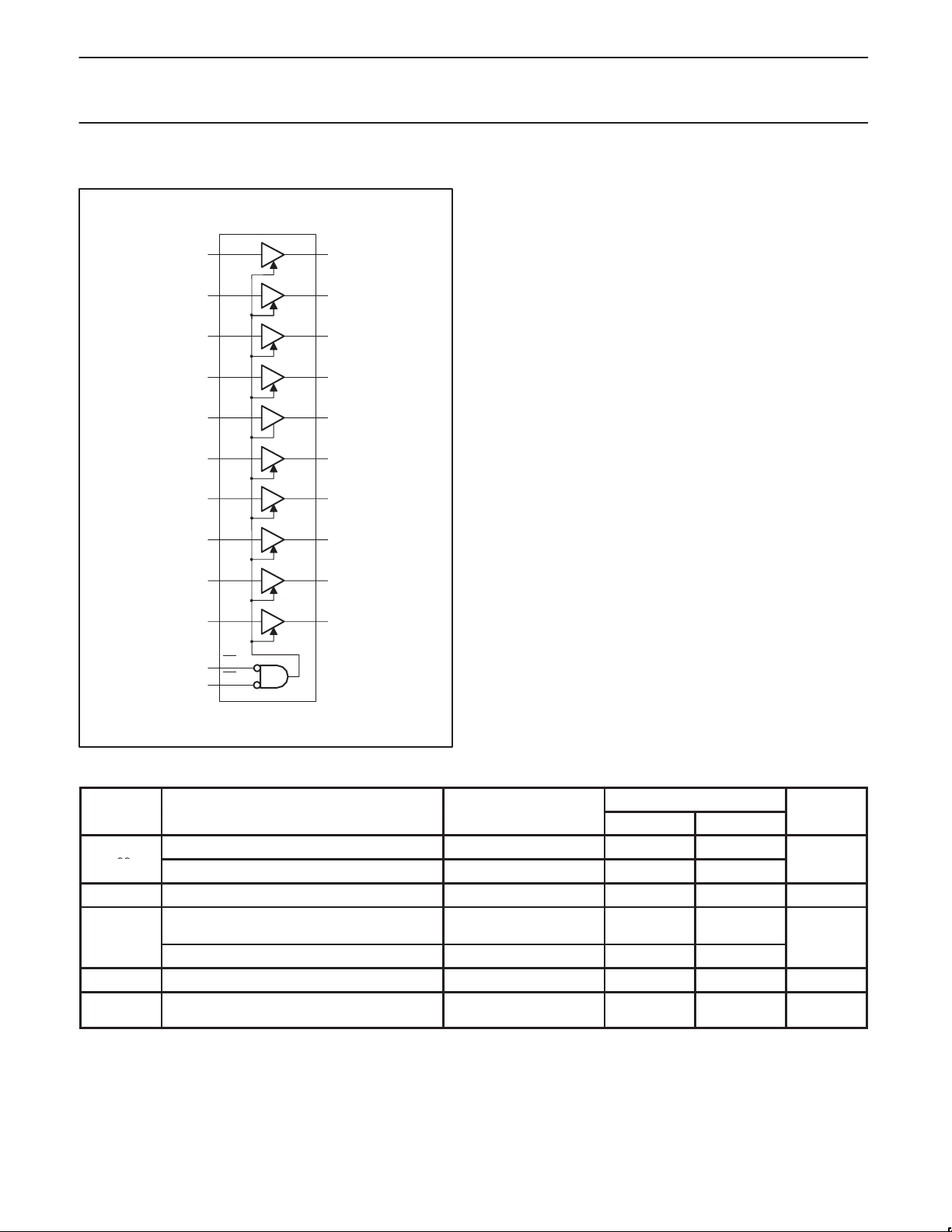
FUNCTIONAL DIAGRAM
A
0
2
A
1
3
A
2
4
A
3
5
A
4
6
A
5
7
A
6
8
A
7
9
Y
0
23
Y
1
22
Y
2
21
Y
3
20
Y
4
19
Y
5
18
Y
6
17
Y
7
16
74LVC827A
A
8
10
A
9
11
OE
1
1
OE
13
2
Y
8
Y
9
SA00429
15
14
RECOMMENDED OPERA TING CONDITIONS
DC supply voltage (for max. speed performance) 2.7 3.6
DC supply voltage (for low-voltage applications) 1.2 3.6
DC Input voltage range 0 5.5 V
I
DC output voltage range; output HIGH or LOW
state
DC output voltage range; output 3-State 0 5.5
Operating ambient temperature range in free-air –40 +85 °C
Input rise and fall times
f
T
CC
V
V
amb
tr, t
VCC = 1.2 to 2.7V
VCC = 2.7 to 3.6V
LIMITS
MIN MAX
0 V
0
0
CC
20
10
V
ns/V
1998 Sep 04
4
 Loading...