

Philips 74LVC823APW, 74LVC823ADB, 74LVC823AD Datasheet

INTEGRATED CIRCUITS
74LVC823A
9-bit D-type flip-flop with 5-volt tolerant
inputs/outputs; positive-edge trigger
(3-State)
Product specification 1998 Sep 24

Philips Semiconductors Product specification
t
L
9-bit D-type flip-flop with 5-volt tolerant
inputs/outputs; positive-edge trigger (3-State)
DESCRIPTION
FEA TURES
•5-volt tolerant inputs/outputs, for interfacing with 5-volt logic
•Supply voltage range of 2.7V to 3.6V
•Complies with JEDEC standard no. 8-1A
•Inputs accept voltages up to 5.5V
•CMOS low power consumption
•Direct interface with TTL levels
•9-bit positive edge-triggered register
•Independent register and 3-State buffer operation
•Flow-through pin-out architecture
The 74LVC823A is a high performance, low-power, low-voltage
Si-gate CMOS device and superior to most advanced CMOS
compatible TTL families.
Inputs can be driven from either 3.3V or 5.0V devices. In 3-state
operation, outputs can handle 5V. This feature allows the use of
these devices as translators in a mixed 3.3V/5V environment.
The 74LVC823A is a 9-bit D-type flip-flop with common clock (CP),
Clock Enable (CE
bus-oriented applications.
The nine flip-flops will store the state of their individual D-inputs that
meet the set-up and hold times requirements on the LOW-to-HIGH
CP transition provided CE
hold their data.
A LOW on MR
When OE
the outputs. When OE
impedance OFF-state. Operation of the OE
state of the flip-flops.
74L VC823A
), Master Reset (MR) and 3-State outputs for
is LOW. When CE is HIGH the flip-flops
resets all flip-flops.
is LOW, the contents of the nine flip-flops is available at
is HIGH, the outputs go to the high
input does not affect the
QUICK REFERENCE DATA
GND = 0 V; T
SYMBOL
NOTES:
is used to determine the dynamic power dissipation (PD in µW)
1. C
PD
P
= CPD × V
D
fi = input frequency in MHz; CL = output load capacity in pF;
f
= output frequency in MHz; VCC = supply voltage in V;
o
(C
L
2. The condition is V
= 25°C; tr = tf ≤ 2.5 ns
amb
PHL/tPLH
f
max
C
I
C
PD
2
× fi (CL × V
CC
2
× V
× fo) = sum of the outputs.
CC
= GND to V
I
PARAMETER CONDITIONS TYPICAL UNIT
Propagation delay
CP to Q
n
Propagation delay
MR to Q
n
Maximum clock frequency
Input capacitance 5.0 pF
Power dissipation capacitance per
flip-flop
2
× fo) where:
CC
CC
CL = 50 pF;
VCC = 3.3 V
CL = 50 pF;
VCC = 3.3 V
Notes 1 and 2 27 pF
5.1 ns
5.2 ns
150 MHz
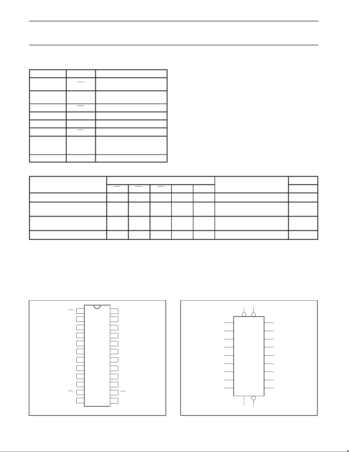
ORDERING INFORMATION
PACKAGES TEMPERATURE RANGE ORDERING CODE PKG. DWG. #
24-Pin Plastic SO –40°C to +85°C 74LVC823A D SOT137-1
24-Pin Plastic SSOP Type II –40°C to +85°C 74LVC823A DB SOT340-1
24-Pin Plastic TSSOP Type I –40°C to +85°C 74LVC823A PW SOT355-1
1998 Sep 24 853-2124 20078
2
Philips Semiconductors Product specification
OPERATING MODES
INTERNAL FLIP-FLOPS
9-bit D-type flip-flop with 5-volt tolerant
inputs/outputs; positive-edge trigger (3-State)
PIN DESCRIPTION
PIN NUMBER SYMBOL NAME AND FUNCTION
1 OE
2, 3, 4, 5, 6,
7, 8, 9, 10
D0 to D8Data inputs
11 MR Master reset (active LOW)
12 GND Ground (0 V)
13 CP Clock pulse (active rising)
14 CE Clock enable (active LOW)
23, 22, 21, 20,
19, 18, 17, 16,
Q0 to Q83-State flip-flop outputs
15
24 V
CC
FUNCTION TABLE
Clear L L X X X L L
Load and read register L
Load register and disable outputs H
Hold L H H NC X NC NC
H = HIGH voltage level
h = HIGH voltage level one set-up time prior to the LOW-to-HIGH
CP transition
L = LOW voltage level
l = LOW voltage level one set-up time prior to the LOW-to-HIGH
CP transition
Z = high impedance OFF-state
↑ = LOW–to–HIGH clock transition
NC= no change
Output enable input
(active LOW)
Positive supply voltage
INPUTS
OE MR CE CP D
L
H
H
H
H
H
L
L
L
L
74LVC823A
OUTPUTS
n
↑
↑
X
X
l
h
l
h
L
H
L
H
Q0 to Q
L
H
Z
Z
8
PIN CONFIGURATION
1998 Sep 24
OE
D
D
D
D
D
D
D
MR
GND
LOGIC SYMBOL
11
1
1
2
D
0
3
D
1
4
2
5
3
6
4
7
5
8
6
9
7
10
8
11
12
24
23
22
21
20
19
18
17
16
15
14
13
SA00418
V
Q
Q
Q
Q
Q
Q
Q
Q
Q
CE
CP
CC
MR
0
1
2
3
4
5
6
7
8
2
3
4
5
6
7
8
9
10
D
0
D
1
D
2
D
3
D
4
D
5
D
6
D
7
D
8
CP CE
13 14
OE
Q
Q
Q
Q
Q
Q
Q
Q
Q
0
1
2
3
4
5
6
7
8
SA00419
23
22
21
20
19
18
17
16
15
3

Philips Semiconductors Product specification
9-bit D-type flip-flop with 5-volt tolerant
inputs/outputs; positive-edge trigger (3-State)
LOGIC SYMBOL (IEEE/IEC)
1
11
14
13
2
3
4
5
6
7
8
9
10
EN
R
G1
1C2
2D
23
22
21
20
19
18
17
16
15
FUNCTIONAL DIAGRAM
2
D
0
3
D
1
4
D
2
5
D
3
D
6
4
FF0 to FF8
D
7
5
D
8
6
D
9
7
D
10
8
CP
13
CE
14
MR
11
OE
1
74LVC823A
3–STATE
OUTPUTS
23
Q
0
22
Q
1
21
Q
2
Q
20
3
Q
19
4
18
Q
5
17
Q
6
16
Q
7
15
Q
8
LOGIC DIAGRAM
MR
CE
CP
OE
SA00420
D
0
D
CP CP CP CP CP CP CP CP CP
D
1
RRRRRRRRR
Q
Q
0
DQ
FF1
D
2
Q
1
DQ
FF2
D
3
Q
2
DQ
FF3
D
4
DQ
Q
3
FF4
D
5
Q
4
DQ
FF5
D
6
DQ
Q
5
FF6
D
7
Q
6
SA00421
D
8
DDQQ
FF7
Q
7
FF8FF0
SA00422
Q
8
1998 Sep 24
4
 Loading...