

Philips 74LVC821APW, 74LVC821ADB, 74LVC821AD Datasheet

INTEGRATED CIRCUITS
74LVC821A
10-bit D-type flip-flop with 5-volt tolerant
inputs/outputs; positive-edge trigger
(3-State)
Product specification 1998 Sep 25
Philips Semiconductors Product specification
V
V
10-bit D-type flip-flop with 5-volt tolerant
inputs/outputs; positive-edge trigger (3-State)
FEA TURES
•5-volt tolerant inputs/outputs, for interfacing with 5-volt logic
•Supply voltage range of 2.7V to 3.6V
•Complies with JEDEC standard no. 8-1A
•Inputs accept voltages up to 5.5V
•CMOS low power consumption
•Direct interface with TTL levels
•10-bit positive edge-triggered register
•Independent register and 3-State buffer operation
•Flow-through pin-out architecture
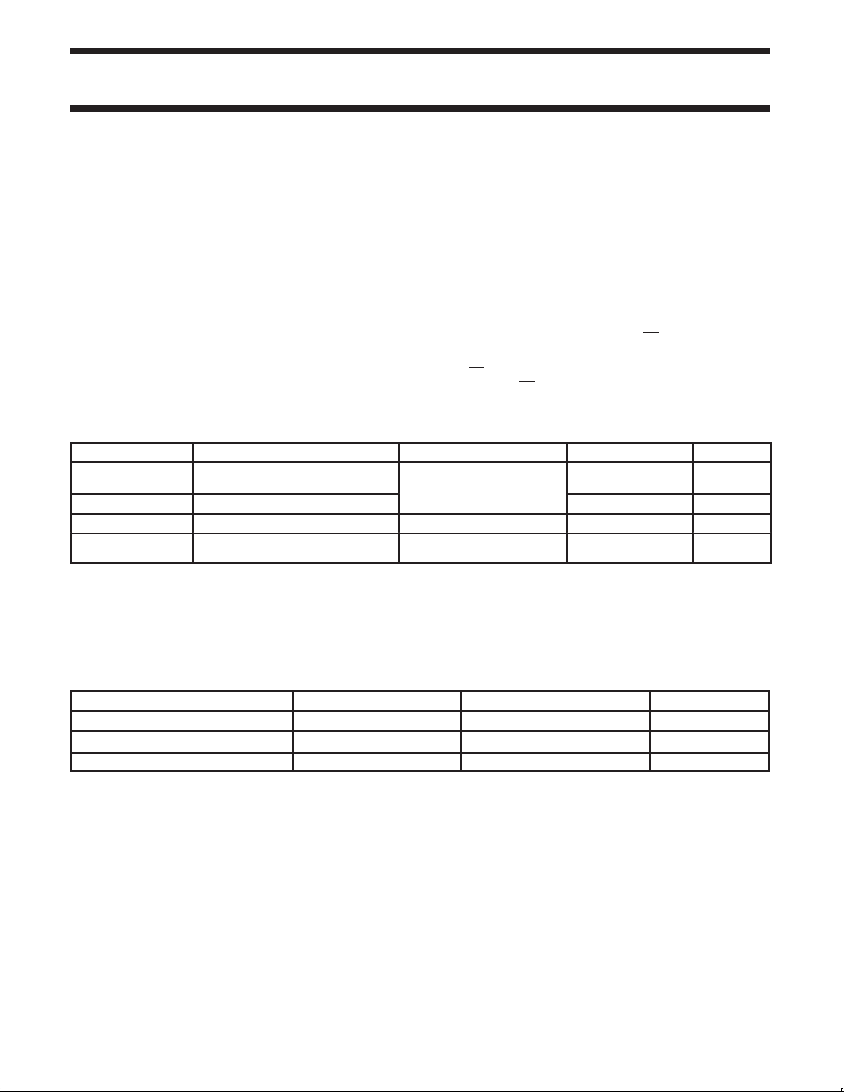
QUICK REFERENCE DATA
GND = 0 V; T
SYMBOL
t
NOTES:
is used to determine the dynamic power dissipation (PD in µW)
1. C
PD
= CPD × V
P
D
f
= input frequency in MHz; CL = output load capacity in pF;
i
= output frequency in MHz; VCC = supply voltage in V;
f
o
(C
L
2. The condition is VI = GND to V
= 25°C; tr = tf ≤ 2.5 ns
amb
PHL/tPLH
f
max
C
I
C
PD
2
× fi (CL × V
CC
2
× V
× fo) = sum of the outputs.
CC
PARAMETER CONDITIONS TYPICAL UNIT
Propagation delay
CP to Q
n
Maximum clock frequency
Input capacitance 5.0 pF
Power dissipation capacitance per
flip-flop
2
× fo) where:
CC
CC
DESCRIPTION
The 74LVC821A is a high performance, low-power, low-voltage
Si-gate CMOS device and superior to most advanced CMOS
compatible TTL families.
Inputs can be driven from either 3.3V or 5.0V devices. In 3-state
operation, outputs can handle 5V. This feature allows the use of
these devices as translators in a mixed 3.3V/5V environment.
The 74LVC821A is a10-bit D-type flip-flop featuring separate D-type
inputs for each flip-flop and 3-State outputs for bus-oriented
applications. A clock (CP) and an output enable (OE
common to all flip-flops. The ten flip-flops will store the state of their
individual D-inputs that meet the set-up and hold times requirements
on the LOW-to-HIGH CP transition. When OE
of the ten flip-flops is available at the outputs.
When OE
Operation of the OE
CL = 50 pF;
= 3.3
CC
Notes 1 and 2 26 pF
74L VC821A
) input are
is LOW, the contents
is HIGH, the outputs go to the high impedance OFF-state.
input does not affect the state of the flip-flops.
5.4 ns
150 MHz
ORDERING INFORMATION
PACKAGES TEMPERATURE RANGE ORDERING CODE PKG. DWG. #
24-Pin Plastic SO –40°C to +85°C 74LVC821A D SOT137-1
24-Pin Plastic SSOP Type II –40°C to +85°C 74LVC821A DB SOT340-1
24-Pin Plastic TSSOP Type I –40°C to +85°C 74LVC821A PW SOT355-1
1998 Sep 25 853-1970 20088
2
Philips Semiconductors Product specification
OPERATING MODES
INTERNAL FLIP-FLOPS
10-bit D-type flip-flop with 5-volt tolerant
inputs/outputs; positive-edge trigger (3-State)
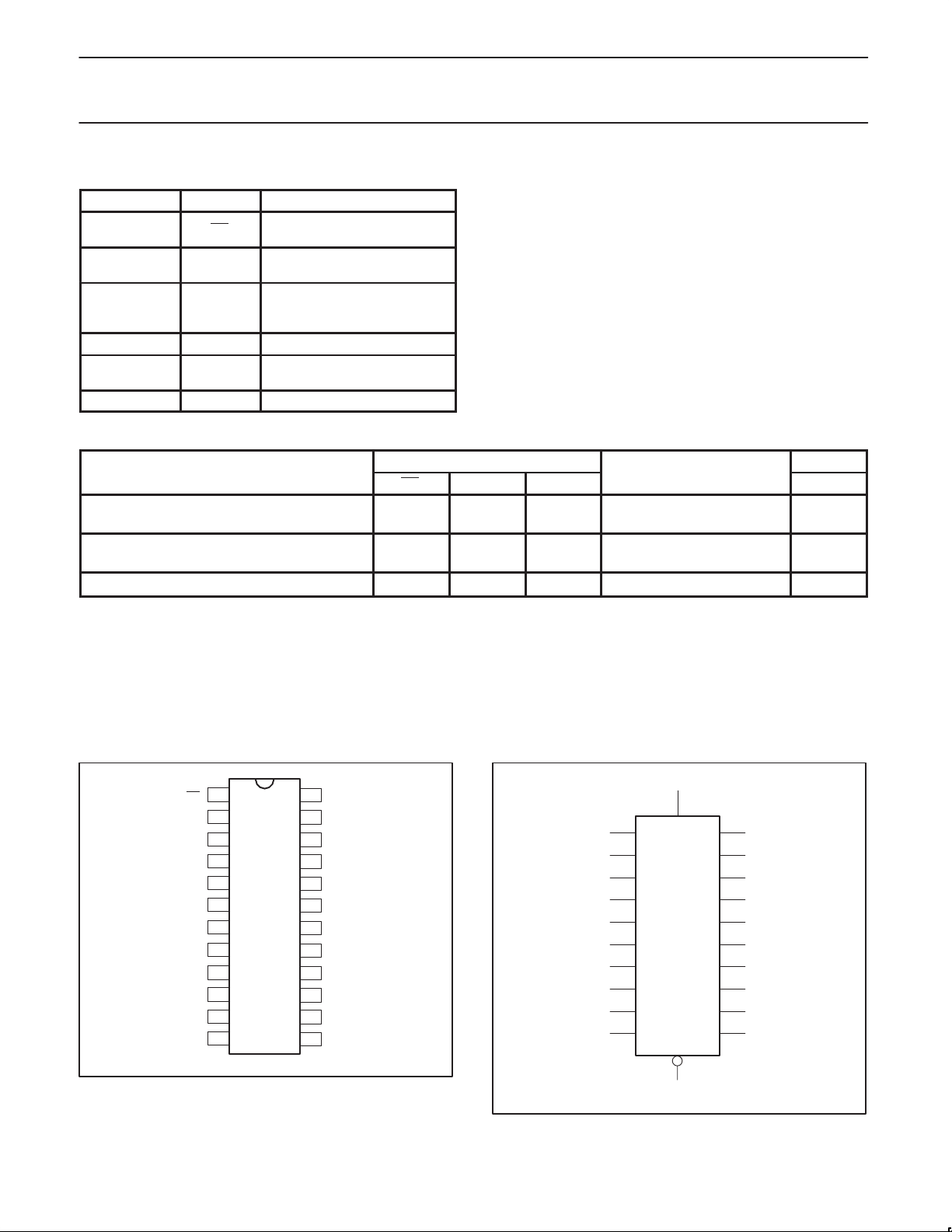
PIN DESCRIPTION
PIN NUMBER SYMBOL NAME AND FUNCTION
1 OE
2, 3, 4, 5, 6,
7, 8, 9, 10, 11
D0 to D9Data inputs
23, 22, 21, 20,
19, 18, 17, 16,
Q0 to Q93-State flip-flop outputs
15, 14
12 GND Ground (0 V)
13 CP
24 V
CC
FUNCTION TABLE
Load and read register L
Load register and disable outputs H
Hold L H or L X NC NC
H = HIGH voltage level
h = HIGH voltage level one set-up time prior to the LOW-to-HIGH
CP transition
L = LOW voltage level
l = LOW voltage level one set-up time prior to the LOW-to-HIGH
CP transition
Z = high impedance OFF-state
↑ = LOW–to–HIGH clock transition
NC= no change
Output enable input
(active LOW)
Clock input (LOW-to-HIGH,
edge-triggered)
Positive supply voltage
OE CP D
INPUTS
↑
L
↑
↑
H
↑
74LVC821A
OUTPUTS
n
l
h
l
h
L
H
L
H
Q0 to Q
L
H
Z
Z
9
PIN CONFIGURATION
1998 Sep 25
OE
D
D
D
D
D
D
D
D
D
D
GND
LOGIC SYMBOL
1
2
0
3
1
4
2
5
3
6
4
7
5
8
6
9
7
10
8
11
9
12
24
23
22
21
20
19
18
17
16
15
14
13
SA00413
V
Q
Q
Q
Q
Q
Q
Q
Q
Q
Q9
CP
CC
0
1
2
3
4
5
6
7
8
2
3
4
5
6
7
8
9
10
11
3
13
CP
D
0
D
1
D
2
D
3
D
4
D
5
D
6
D
7
D
8
D
9
Q
Q
Q
Q
Q
Q
Q
Q
Q
Q
OE
1
0
1
2
3
4
5
6
7
8
9
SA00414
23
22
21
20
19
18
17
16
15
14

Philips Semiconductors Product specification
10-bit D-type flip-flop with 5-volt tolerant
inputs/outputs; positive-edge trigger (3-State)
LOGIC SYMBOL (IEEE/IEC)
13
1
2
3
4
5
6
7
8
9
10
11
C1
EN
1D
23
22
21
20
19
18
17
16
15
14
FUNCTIONAL DIAGRAM
2
D
0
3
D
1
4
D
2
5
D
3
6
D
4
7
D
8
D
9
D
10
D
11
D
CP
13
1
OE
FF0 to FF9
5
6
7
8
9
74LVC821A
3–STATE
OUTPUTS
23
Q
0
22
Q
1
21
Q
2
20
Q
3
Q
19
4
18
Q
5
17
Q
6
16
Q
7
15
Q
8
14
Q
9
LOGIC DIAGRAM
D
0
D
CP CP CP CP CP CP CP CP CP CP
FF0
CP
OE
Q
D
8
SA00416
9
Q
SA00417
9
SA00415
D
1
Q
Q
DQ
0
FF1
Q
D
2
1
DQ
FF2
Q
D
3
2
DQ
FF3
Q
D
3
4
DQ
FF4
Q
D
5
4
DQ
FF5
Q
D
6
5
DQ
FF6
D
7
DDDQQQ
Q
6
D
8
FF7 FF8 FF9
Q
7
1998 Sep 25
4
 Loading...