

Philips 74LVC652PW, 74LVC652DB, 74LVC652D Datasheet

INTEGRATED CIRCUITS
74LVC652
Octal transceiver/register with dual
enable (3-State)
Product specification
Supercedes data of 1993 Dec 01
IC24 Data Handbook
1998 Jul 29

Philips Semiconductors Product specification
Octal transceiver/register with dual enable (3-State)
*FEA TURES
•Wide supply voltage range of 1.2V to 3.6V
•In accordance with JEDEC standard no. 8-1A
•CMOS low power consumption
•Direct interface with TTL levels
•5 Volt tolerant inputs/outputs, for interfacing with 5 Volt logic
DESCRIPTION
The 74LVC652 is a high performance, low-power, low-voltage
Si-gate CMOS device, superior to most advanced CMOS
compatible TTL families.
Inputs can be driven from either 3.3V or 5.0V devices. In 3-State
operation, outputs can handle 5V. This feature allows the use of
these devices as translators in a mixed 3.3V/5V environment.
QUICK REFERENCE DATA
GND = 0V; T
SYMBOL
t
PHL/tPLH
f
max
C
I
C
PD
NOTES:
1. C
is used to determine the dynamic power dissipation (PD in µW)
PD
= CPD V
P
D
f
= input frequency in MHz; CL = output load capacitance in pF;
i
= output frequency in MHz; VCC = supply voltage in V;
f
o
Σ (C
L
2. The condition is V
= 25°C; tr = tf 2.5 ns
amb
2
x fi Σ (CL V
CC
2
V
fo) = sum of the outputs.
CC
= GND to V
I
PARAMETER CONDITIONS TYPICAL UNIT
Propagation delay
An to Bn; Bn to A
Maximum clock frequency 150 MHz
Input capacitance 5.0 pF
Power dissipation capacitance per latch Notes 1, 2 45 pF
CC.
n
2
fo) where:
CC
The 74LVC652 consist of 8 non-inverting bus transceiver circuits
with 3-State outputs, D-type flip-flops and control circuitry arranged
for multiplexed transmission of data directly from the internal
registers. Data on the ‘A’ or ‘B’ or both buses, will be stored in the
internal registers, at the appropriate clock inputs (CPAB or CPBA)
regardless of the select inputs (SAB and SBA) or output enable
(OEAB and OE
SAB and SBA data can directly go from input to output (real time
mode) or data can be controlled by the clock (storage mode), this is
when the OEn inputs this operating mode permits. The output
enable inputs OEAB and OEBA determine the operation mode of
the transceiver.
When OEAB is LOW, no data transmission from An to Bn is possible
and when OE
An possible. When SAB and SBA are in the real time transfer mode,
it is also possible to store data without using the internal D-type
flip-flops by simultaneously enabling OEAB and OE
configuration each output reinforces its input.
CL = 50pF
VCC = 3.3V 5.0
BA) control inputs. Depending on the select inputs
BA is HIGH, there is no data transmission from Bn to
74L VC652
BA. In this
ns
ORDERING AND PACKAGE INFORMA TION
PACKAGES TEMPERATURE RANGE
24-Pin Plastic SO –40°C to +85°C 74LVC652 D 74LVC652 D SOT137-1
24-Pin Plastic SSOP Type II –40°C to +85°C 74LVC652 DB 74LVC652 DB SOT340-1
24-Pin Plastic TSSOP Type I –40°C to +85°C 74LVC652 PW 4LVC652PW DH SOT355-1
1998 Jul 29 853-2104 19803
OUTSIDE NORTH
AMERICA
2
NORTH AMERICA PKG. DWG. #

Philips Semiconductors Product specification
FUNCTION
74LVC652Octal transceiver/register with dual enable (3-State)
PIN CONFIGURATION
PIN DESCRIPTION
PIN NUMBER SYMBOL FUNCTION
1 CP
CP
OE
S
GND
AB
AB
AB
1
2
3
A
4
0
5
A
1
A
6
2
A
7
3
A
8
4
9
A
5
10
A
6
A
11
7
12
V
24
CP
23
S
22
OE
21
B
20
19
B
B
18
B
17
B
16
B
15
B
14
B
13
SV00767
CC
BA
0
1
2
3
4
5
6
7
BA
BA
2 S
3 OE
4, 5, 6, 7, 8,
9, 10, 11
12 GND Ground (0V)
20, 19, 18, 17,
16, 15, 14, 13
21 OE
22 S
23 CP
24 V
FUNCTION TABLE
INPUTS DATA I/O *
OE
* The data output functions may be enabled or disabled by
various signals at the OE
functions are always enabled, i.e., data at the bus inputs will
be stored on every LOW-to-HIGH transition on the clock
inputs.
un = unspecified
H = HIGH voltage level
L = LOW voltage level
X = Don’t care
↑ = LOW–to–HIGH level transition
OE
AB
L
L
X
H
L
L
L
L
H
H
BA
H
H
H
H
X
L
L
L
H
H
CP
AB
CP
BA
H or L↑H or L
↑
↑
H or L
↑
H or L
↑
X
X
X
H or L
↑
↑
↑
X
H or L
X
X
S
AB
X
X
X
L
X
X
X
X
L
H
S
BA
X
X
X
X
X
L
L
H
X
X
A0 to A
7
input input
input
input
un *
output
output input
input output
H L H or L H or L H H output output
and OEBA inputs. Data input
AB
B0 to B
un *
output
input
input
7
AB
AB
AB
A0 to A
B0 to B
BA
BA
BA
CC
‘A’ to ‘B’ clock input
(LOW-to-HIGH, edge-triggered)
Select ‘A’ to ‘B’ source input
Output enable B to A input
(active LOW)
‘A’ data inputs/outputs
7
‘B’ data inputs/outputs
7
Output enable A to B input
Select ‘B’ to ‘A’ source input
‘B’ to ‘A’ clock input
(LOW-to-HIGH, edge-triggered)
Positive supply voltage
isolation
store A and B data
store A, hold B,
store A in both registers
hold A, store B,
store B in both registers
real-time B data to A bus
stored B data to A bus
real-time A data to B bus
stored A data to B bus
stored A data to B bus and
stored B data to A bus
1998 Jul 29
3

Philips Semiconductors Product specification
74LVC652Octal transceiver/register with dual enable (3-State)
LOGIC SYMBOL
1
2
4
5
6
7
8
9
10
11
AB
S
AB
A
0
A
1
A
2
A
3
A
4
A
5
A
6
A
7
OE
OE
CP
LOGIC SYMBOL (IEEE/IEC)
23
1
22
2
21
3
C4
C5
G6
G7
3EN1
3EN2
BA
AB
FUNCTIONAL DIAGRAM
21
CP
S
3
BA
BA
B
0
B
1
B
2
B
3
B
4
B
5
B
6
B
7
SV00768
23
22
20
19
18
17
16
15
14
13
4
A
0
A
5
1
A
6
2
A
7
3
A
8
4
A
9
5
A
10
6
A
11
7
21
OE
BA
3
OE
AB
2
S
AB
22
S
BA
1
CP
AB
23
CP
BA
B
B
B
B
B
B
B
B
0
1
2
3
4
5
6
7
20
19
18
17
16
15
14
13
SV00770
4
5
6
7
8
9
10
11
1998 Jul 29
1
6
1
6
5D
1
4D
1
1
7
2
7
20
19
18
17
16
15
14
13
SV00769
4
Philips Semiconductors Product specification
74LVC652Octal transceiver/register with dual enable (3-State)
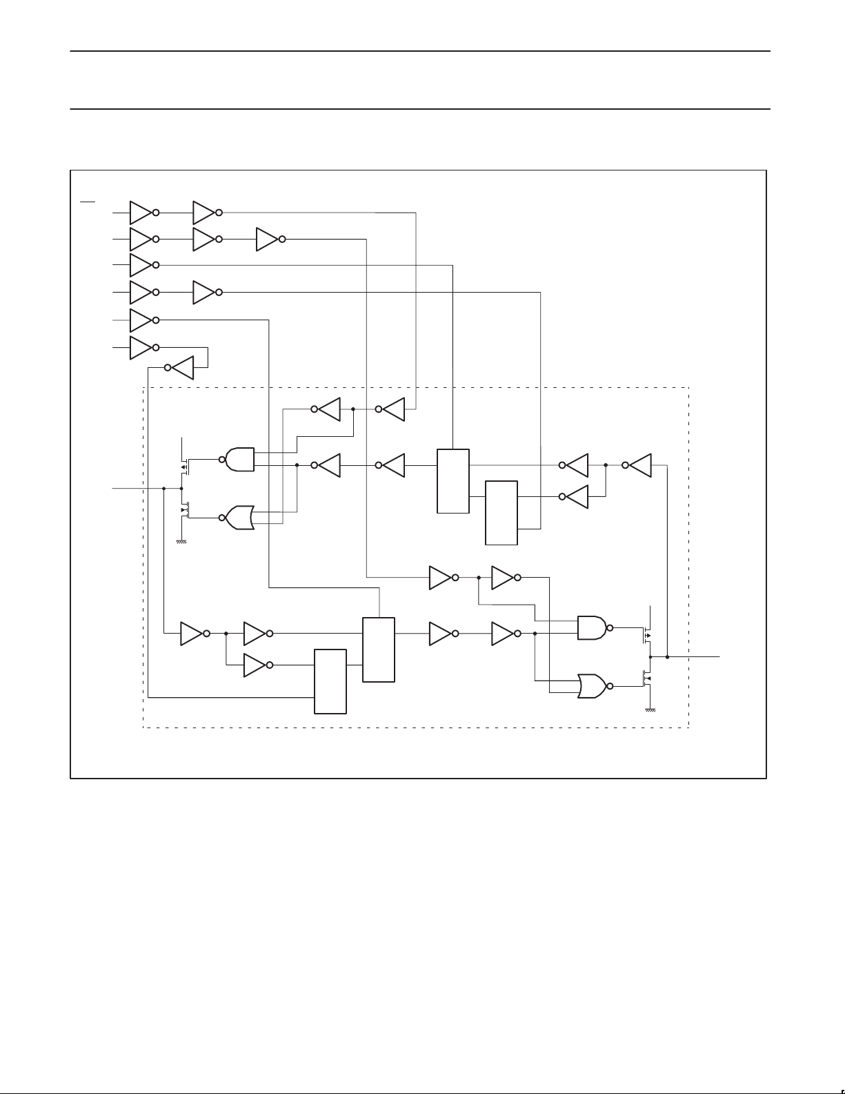
LOGIC DIAGRAM
OE
BA
OE
AB
S
BA
CP
BA
S
AB
CP
AB
V
CC
S
D
Y
1
A
n
S
D
Y
1
MUX
D
Q
D
FF
CP
8 identical channels
2
n
MUX
D
2
D
Q
FF
n
CP
V
CC
B
n
SV00771
1998 Jul 29
5
 Loading...