

Philips 74LVC623APW, 74LVC623ADB, 74LVC623AD Datasheet

INTEGRATED CIRCUITS
74LVC623A
Octal transceiver with dual enable
(3-State)
Product specification 1998 Jul 29
Philips Semiconductors Product specification
74L VC623AOctal transceiver with dual enable (3-State)
FEA TURES
•Wide supply voltage range of 1.2V to 3.6V
•In accordance with JEDEC standard no. 8-1A
•Flow-through pin-out architecture
•CMOS low power consumption
•Inputs accept voltages up to 5.5V
•Direct interface with TTL levels
•Output drive capability 50 transmission lines @ 85°C
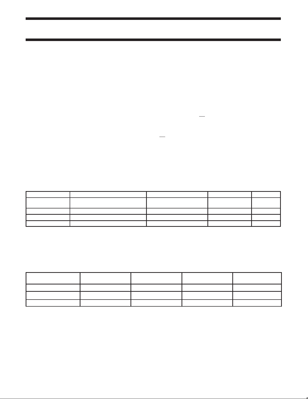
QUICK REFERENCE DATA
GND = 0V; T
SYMBOL
t
PHL/tPLH
C
I
C
I/O
C
PD
NOTES:
1. C
is used to determine the dynamic power dissipation (PD in µW)
PD
= CPD V
P
D
f
= input frequency in MHz; CL = output load capacity in pF;
i
= output frequency in MHz; VCC = supply voltage in V;
f
o
Σ (C
L
2. The condition is V
= 25°C; tr = tf 2.5 ns
amb
2
x fi Σ (CL V
CC
2
V
fo) = sum of the outputs.
CC
= GND to V
I
PARAMETER CONDITIONS TYPICAL UNIT
Propagation delay
An to Bn; Bn to An
Input capacitance 5.0 pF
Input/output capacitance 10 pF
Power dissipation capacitance per latch Notes 1, 2 32 pF
2
fo) where:
CC
CC.
DESCRIPTION
The 74LVC623A is a high performance, low-power, low-voltage
Si-gate CMOS device, superior to most advanced CMOS
compatible TTL families.
The 74LVC623A is an octal transceiver featuring non-inverting
3-State bus compatible outputs in both send and receive directions.
This octal bus transceiver is designed for asynchronous two-way
communication between data buses.
The control function implementation allows maximum flexibility in
timing. This device allows data transmission from the A bus to the B
bus or from the B bus to the A bus, depending upon the levels at the
enable inputs (OEAB, OE
disable the device so that the buses are effectively isolated. The
dual enable function configuration gives this transceiver the
capability to store data by simultaneous enabling of OEAB and
OE
BA. Each output reinforces its input in this transceiver
configuration. Thus, when both control inputs are enabled and all
other data sources to the two sets of the bus lines are at high
impedance OFF-state, both sets of bus lines will remain at their last
states. The 8-bit codes appearing on the two sets of buses will be
identical.
The ‘623A’ is identical to the ‘620A’ but has true (non-inverting)
outputs.
CL = 50pF
VCC = 3.3V 3.3
BA). The enable inputs can be used to
ns
ORDERING AND PACKAGE INFORMA TION
PACKAGES TEMPERATURE RANGE
20-Pin Plastic SO –40°C to +85°C 74LVC623A D 74LVC623A D SOT163-1
20-Pin Plastic SSOP Type II –40°C to +85°C 74LVC623A DB 74LVC623A DB SOT339-1
20-Pin Plastic TSSOP Type I –40°C to +85°C 74LVC623A PW 7LVC623APW DH SOT360-1
1998 Jul 29 853-2106 19803
OUTSIDE NORTH
AMERICA
2
NORTH AMERICA PKG. DWG. #
Philips Semiconductors Product specification
74LVC623AOctal transceiver with dual enable (3-State)
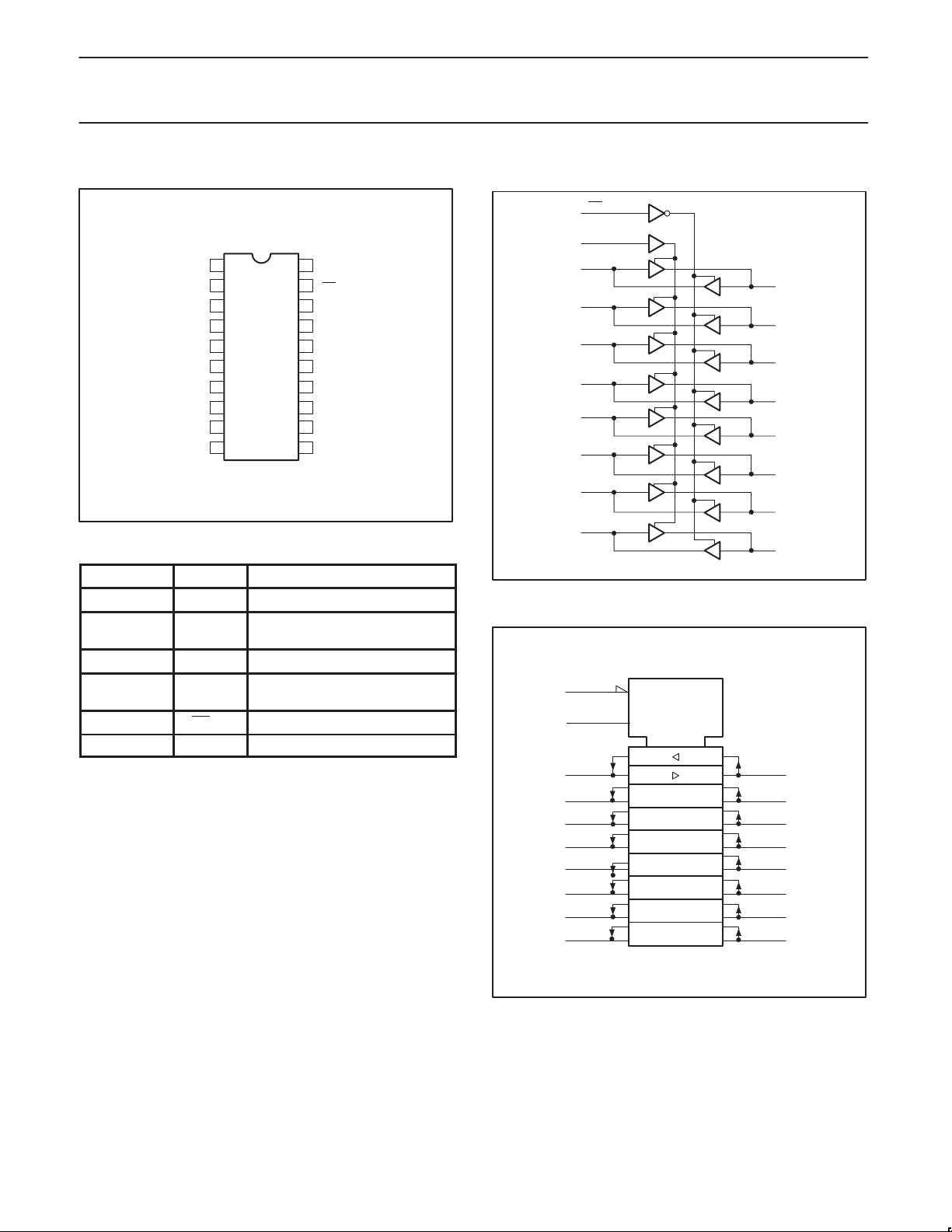
PIN CONFIGURATION
1
OEAB
2
A0
3
A1
4
A2
5
A3
6
A4
7
A5
8
A6
9
A7
10 11
GND
20
V
19
OEBA
18
B0
17
B1
16
B2
15
B3
14
B4
13
B5
12
B6
B7
SV00744
CC
PIN DESCRIPTION
PIN NUMBER SYMBOL NAME AND FUNCTION
1 OEAB Direction control
2, 3, 4, 5,
6, 7, 8, 9
10 GND Ground (0V)
18, 17, 16, 15,
14, 13, 12, 11
19 OEBA Output enable input (active LOW)
20 V
A0 – A7 Data inputs/outputs
B0 – B7 Data inputs/outputs
CC
Positive supply voltage
LOGIC SYMBOL
BA
OE
19
OEAB
1
A0
2
A1
3
A2
4
A3
5
A4
6
A5
7
A6
8
A7
9
LOGIC SYMBOL (IEEE/IEC)
19
1
2
3
4
5
6
7
8
9
EN1
EN2
∇ 1
2 ∇
B0
B1
B2
B3
B4
B5
B6
B7
SV00745
18
17
16
15
14
13
12
11
18
17
16
15
14
13
12
11
1998 Jul 29
SV00746
3
 Loading...