

Philips 74LVC574APW, 74LVC574ADB, 74LVC574AD Datasheet
INTEGRATED CIRCUITS
74LVC574A
Octal D-type flip-flop with 5-volt tolerant
inputs/outputs; positive edge-trigger
(3-State)
Product specification 1998 Jul 29
Philips Semiconductors Product specification
Octal D-type flip-flop with 5-volt tolerant
inputs/outputs; positive edge-trigger (3-State)
FEA TURES
•5-volt tolerant inputs/outputs, for interfacing with 5-volt logic
•Supply voltage range of 2.7V to 3.6V
•Complies with JEDEC standard no. 8-1A
•Inputs accept voltages up to 5.5V
•CMOS low power consumption
•Direct interface with TTL levels
•High impedance when V
CC
= 0V
•8-bit positive edge-triggered register
•Independent register and 3-State buffer operation
•Flow-through pin-out architecture
DESCRIPTION
The 74LVC574A is a high-performance, low-power, low-voltage,
Si-gate CMOS device, superior to most advanced CMOS
compatible TTL families.
Inputs can be driven from either 3.3V or 5V devices. In 3-State
operation, outputs can handle 5V. This feature allows the use of
these devices as translators in a mixed 3.3V/5V environment.
The 74LVC574A is an octal D-type flip-flop featuring separate
D-type inputs for each flip-flop and 3-State outputs for bus-oriented
applications. A clock (CP) and an output enable (OE
common to all flip-flops.
The eight flip-flops will store the state of their individual D-inputs
that meet the setup and hold times requirements on the
LOW-to-HIGH CP transition.
When OE
the outputs. When OE
impedance OFF-state. Operation of the OE
state of the flip-flops.
The ’574A’ is functionally identical to the ’374A’, but the ’374A’ has a
different pin arrangement.
74L VC574A
) input are
is LOW, the contents of the eight flip-flops is available at
is HIGH, the outputs go to the high
input does not affect the
QUICK REFERENCE DATA
GND = 0V; T
SYMBOL
t
PHL/tPLH
f
max
C
I
C
PD
NOTE:
is used to determine the dynamic power dissipation (PD in W):
1. C
PD
= CPD x V
P
D
f
= input frequency in MHz; CL = output load capacity in pF;
i
= output frequency in MHz; VCC = supply voltage in V;
f
o
(C
2. The condition is V
=25°C; tr = tf 2.5ns
amb
2
CC
2
x V
x fo) = sum of outputs.
L
CC
PARAMETER CONDITIONS TYPICAL UNIT
Propagation delay
CP to Q
n
maximum clock frequency 150 MHz
Input capacitance 5.0 pF
Power dissipation capacitance per
flip-flop
x fi + (CL x V
= GND to V
I
CC
CC
2
x fo) where:
CL = 50pF
V
= 3.3V 4.8
CC
Notes 1 and 2 20 pF
ns
ORDERING INFORMATION
PACKAGES
20-Pin Plastic Shrink Small Outline (SO) –40°C to +85°C 74LVC574A D 74LVC574A D SOT163-1
20-Pin Plastic Shrink Small Outline (SSOP) Type II –40°C to +85°C 74LVC574A DB 74LVC574A DB SOT339-1
20-Pin Plastic Thin Shrink Small Outline (TSSOP) Type I –40°C to +85°C 74LVC574A PW 7LVC574APW DH SOT360-1
TEMPERATURE
RANGE
OUTSIDE
NORTH AMERICA
NORTH AMERICA PKG. DWG. #
1998 Jul 29 853-1863 19804
2
Philips Semiconductors Product specification
Octal D-type flip-flop with 5-volt tolerant
inputs/outputs; positive edge-trigger (3-State)
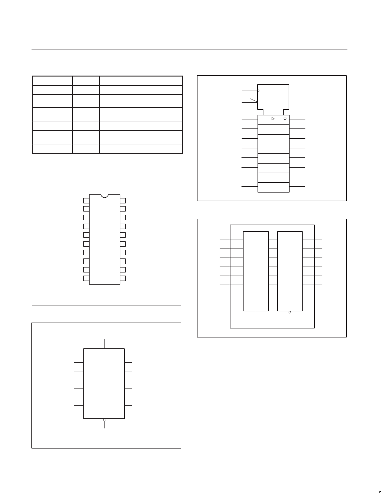
PIN DESCRIPTION
PIN NUMBER SYMBOL FUNCTION
1 OE Output enable input (active-Low)
2, 3, 4, 5,
6, 7, 8, 9
19, 18, 17, 16,
15, 14, 13, 12
10 GND Ground (0V)
11 CP
20 V
PIN CONFIGURATION
D0-D7 Data inputs
Q0-Q7 Data outputs
Clock input (LOW-to-HIGH,
edge-triggered)
Positive supply voltage
CC
1
OE
2
D0
3
D1
4
D2
5
D3
D4
6
D5
7
D6
8
D7
9
GND
10 11
SA00400
20
V
CC
19
Q0
18
Q1
17
Q2
16
Q3
15
Q4
14
Q5
13
Q6
12
Q7
CP
LOGIC SYMBOL (IEEE/IEC)
1
C1
11
EN
2
1D
3
4
5
6
7
8
9
FUNCTIONAL DIAGRAM
2
D0
318
D1 Q1
516
D3 Q3
FF!
6
714
912
to
FF8
D5 Q5
D7 Q7
74LVC574A
19
18
17
16
15
14
13
12
SA00402
Q0
Q2D2
3-State
OUTPUTS
Q4D4
Q6D6
19
174
15
138
LOGIC SYMBOL
2
3
4
5
6
7
8
9
1998 Jul 29
CP
11
1
OE
11
CP
D0
D1
D2
D3
D4
D5
D6
D7
OE
1
Q0
Q1
Q2
Q3
Q4
Q5
Q6
Q7
19
18
17
16
15
14
13
12
SA00401
SA00403
3
 Loading...