

Philips 74lvc573a DATASHEETS
INTEGRATED CIRCUITS
74LVC573A
Octal D-type transparent latch with 5-volt
tolerant inputs/outputs (3-State)
Product specification 1998 Jul 29
Philips Semiconductors Product specification
Octal D-type transparent latch with 5-volt
tolerant inputs/outputs (3-State)
FEA TURES
•5-volt tolerant inputs/outputs, for interfacing with 5-volt logic
•Supply voltage range of 2.7V to 3.6V
•Complies with JEDEC standard no. 8-1A
•Inputs accept voltages up to 5.5V
•CMOS low power consumption
•Direct interface with TTL levels
•High impedance when V
•Flow-through pin-out architecture
DESCRIPTION
The 74LVC573A is a high-performance, low-power, low-voltage,
Si-gate CMOS device, superior to most advanced CMOS
compatible TTL families.
Inputs can be driven from either 3.3V or 5V devices. In 3-State
operation, outputs can handle 5V. This feature allows the use of
these devices as translators in a mixed 3.3V/5V environment.
CC
= 0V
74L VC573A
The 74LVC573A is an octal D-type transparent latch featuring
separate D-type inputs for each latch and 3-State outputs for
bus-oriented applications. A latch enable (LE) input and an output
enable (OE
The ’573A’ consists of eight D-type transparent latches with 3-State
true outputs. When LE is HIGH, data at the D
latches. In this condition, the latches are transparent, i.e. a latch
output will change each time its corresponding D-input changes.
When LE is LOW, the latches store the information that was present
at the D-inputs one setup time preceding the HIGH-to-LOW
transition of LE. When OE
are available at the outputs. When OE
high impedance OFF-state. Operation of the OE
affect the state of the latches.
The ’573A’ is functionally identical to the ’373A’, but the ’373A’ has a
different pin arrangement.
) input are common to all internal latches.
inputs enters the
n
is LOW, the contents of the eight latches
is HIGH, the outputs go to the
input does not
QUICK REFERENCE DATA
SYMBOL PARAMETER CONDITIONS TYPICAL UNIT
t
PHL/tPLH
C
I
C
PD
NOTE:
is used to determine the dynamic power dissipation (PD in W):
1. C
PD
= CPD x V
P
D
= input frequency in MHz; CL = output load capacity in pF;
f
i
= output frequency in MHz; VCC = supply voltage in V;
f
o
(C
L
2. The condition is V
CC
2
x V
x fo) = sum of outputs.
CC
Propagation delay
Dn to Q
n;
LE to Q
n
Input capacitance 5.0 pF
Power dissipation capacitance per latch Notes 1 and 2 20 pF
2
x fi + (CL x V
= GND to V
I
CC
CC
2
x fo) where:
CL = 50pF
VCC = 3.3V 4.3
4.6
ns
ORDERING INFORMATION
PACKAGES
20-Pin Plastic Shrink Small Outline (SO) –40°C to +85°C 74LVC573A D 74LVC573A D SOT163-1
20-Pin Plastic Shrink Small Outline (SSOP) Type II –40°C to +85°C 74LVC573A DB 74LVC573A DB SOT339-1
20-Pin Plastic Thin Shrink Small Outline (TSSOP) Type I –40°C to +85°C 74LVC573A PW 7LVC573APW DH SOT360-1
TEMPERATURE
RANGE
OUTSIDE
NORTH AMERICA
NORTH AMERICA PKG. DWG. #
1998 Jul 29 853-1862 19804
2
Philips Semiconductors Product specification
Octal D-type transparent latch with 5-volt
tolerant inputs/outputs (3-State)
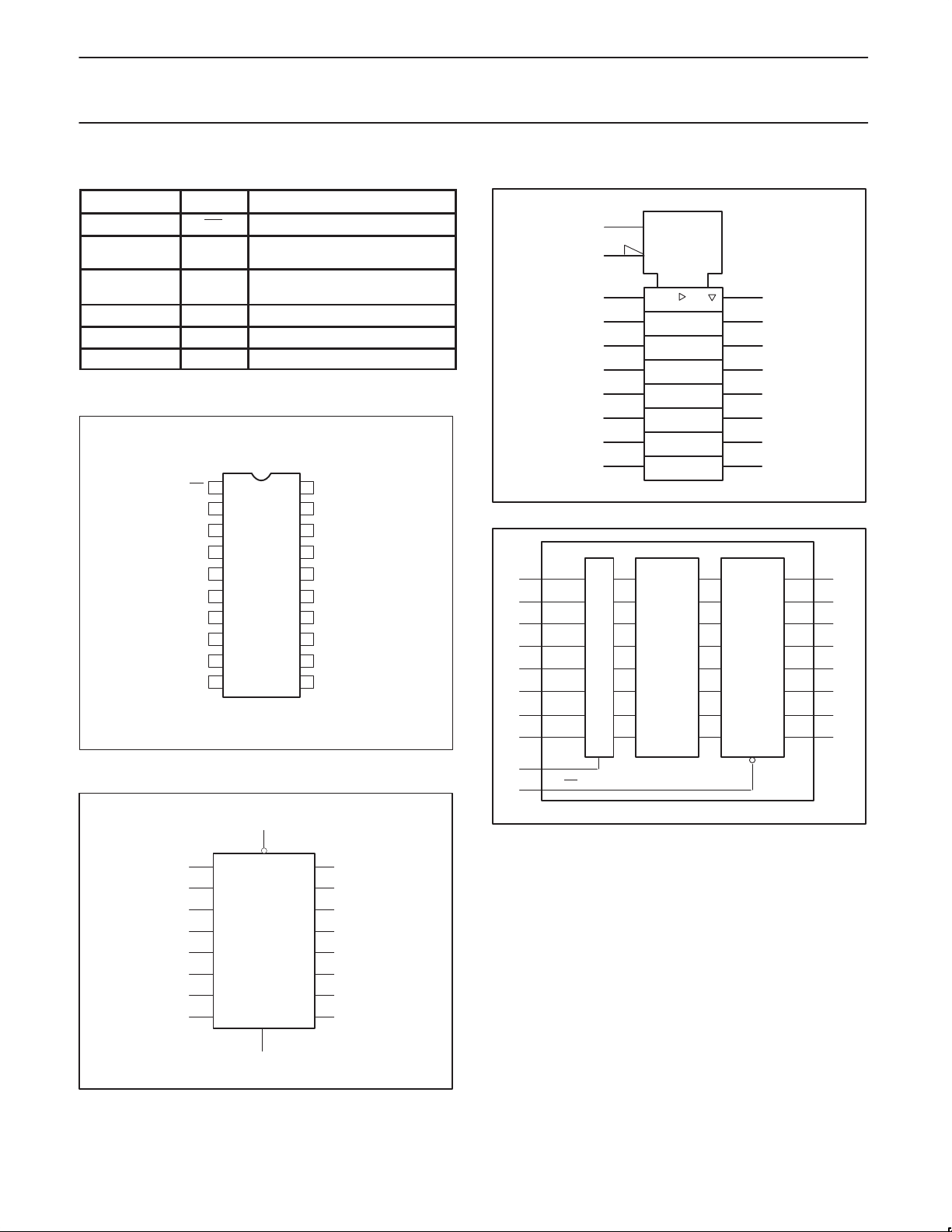
PIN DESCRIPTION
PIN NUMBER SYMBOL FUNCTION
1 OE Output enable input (active-Low)
2, 3, 4, 5,
6, 7, 8, 9
19, 18, 17, 16,
15, 14, 13, 12
10 GND Ground (0V)
11 LE Latch enable input (active-High)
20 V
PIN CONFIGURATION
D0-D7 Data inputs
Q0-Q7 Data outputs
Positive supply voltage
CC
OE
1
2
D0
3
D1
4
D2
5
D3
D4
6
D5
7
D6
8
D7
9
GND
10 11
SA00395
20
V
CC
19
Q0
18
Q1
17
Q2
16
Q3
15
Q4
14
Q5
13
Q6
12
Q7
LE
74LVC573A
LOGIC SYMBOL (IEEE/IEC)
11
C1
1
EN1
2
1D
3
4
5
6
7
8
9
FUNCTIONAL DIAGRAM
318
D1 Q1
516
D3 Q3
6
714
D5 Q5
912
D7 Q7
LATCH
1 to 8
19
18
17
16
15
14
13
12
SA00397
3-State
OUTPUTS
192
Q0D0
174
Q2D2
15
Q4D4
138
Q6D6
LOGIC SYMBOL
2
3
4
5
6
7
8
9
1998 Jul 29
LE
11
1
OE
1
OE
D0
D1
D2
D3
D4
D5
D6
D7
LE
11
Q0
Q1
Q2
Q3
Q4
Q5
Q6
Q7
19
18
17
16
15
14
13
12
SA00396
SA00398
3
Philips Semiconductors Product specification
OPERATING MODES
INTERNAL LATCHES
Octal D-type transparent latch with 5-volt
tolerant inputs/outputs (3-State)
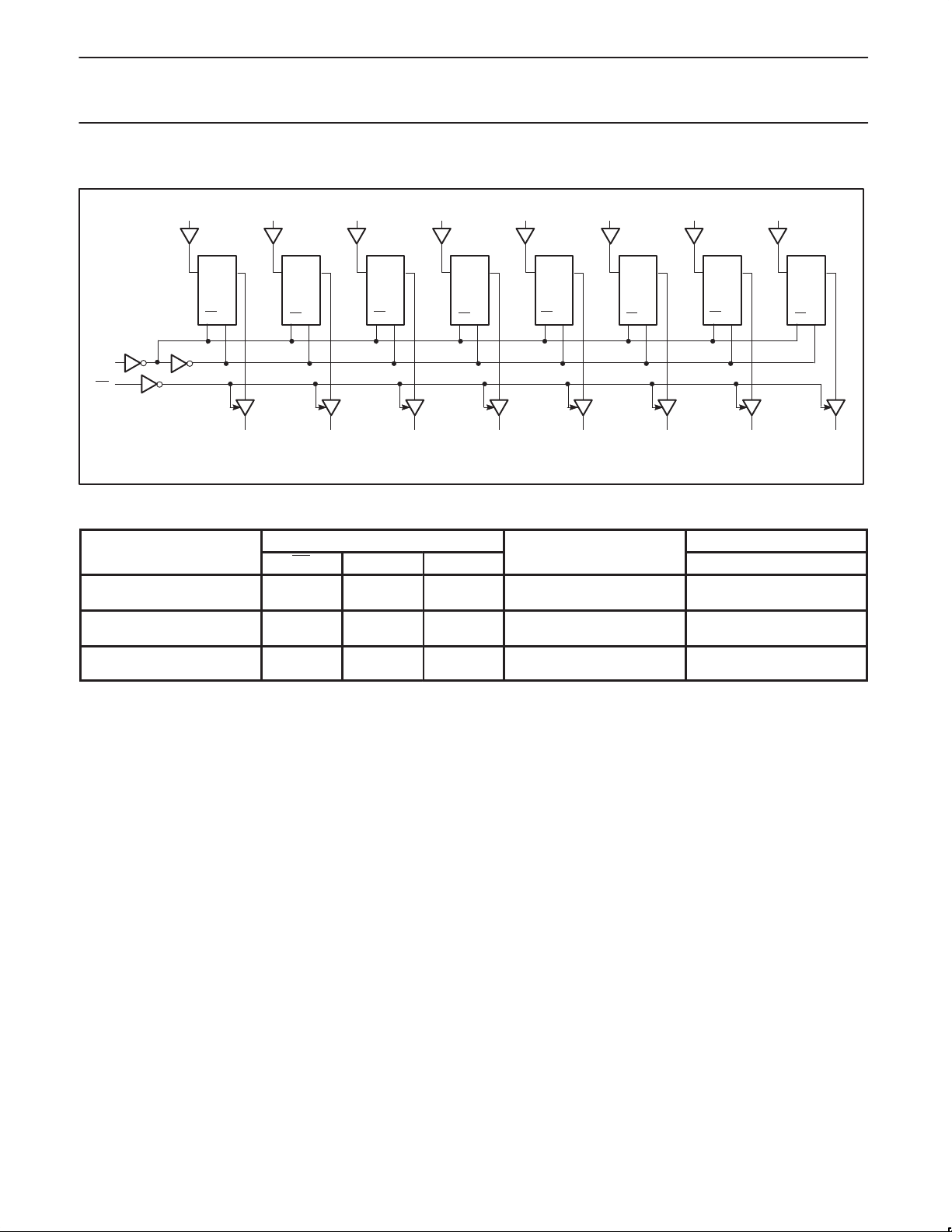
LOGIC DIAGRAM
D0
D
LATCH
1
LE
LE
LE
OE
FUNCTION TABLE
Enable and read register
(transparent mode)
Latch and read register L
Latch register and
disable outputs
H = HIGH voltage level
h = HIGH voltage level one setup time prior to the HIGH-to-LOW LE transition
L = LOW voltage level
l = LOW voltage level one setup time prior to the HIGH-to-LOW LE transition
X = Don’t care
Z = High impedance OFF-state
D1
Q
Q0 Q1 Q2 Q3 Q4 Q5 Q6 Q7
D
LATCH
2
LE
LE
D2
QQQ QQQQ
D
LATCH
3
LE
LE
D3
D
LATCH
4
LE
LE
INPUTS
OE LE D
L
L
H
H
L
L
H
H
L
L
L
n
L
H
l
h
l
h
D4
D
LATCH
5
LE
74LVC573A
D5
D
LATCH
6
LE
LE
LE
L
H
L
H
L
H
D6
D
LATCH
7
LE
LE
OUTPUTS
Q0 to Q
D7
D
LATCH
8
LE
LE
SA00399
7
L
H
L
H
Z
Z
1998 Jul 29
4
 Loading...