

Philips 74lvc544a DATASHEETS

INTEGRATED CIRCUITS
74LVC544A
Octal D-type registered transceiver,
inverting (3-State)
Product specification 1998 Jul 29
Philips Semiconductors Product specification
Octal D-type registered transceiver, inverting
(3-State)
FEA TURES
•Wide supply voltage range of 1.2V to 3.6V
•In accordance with JEDEC standard no. 8-1A
•CMOS low power consumption
•Direct interface with TTL levels
•Combines 74L VC640 and 74LVC533 type functions in one chip
•Octal transceiver with D-type latch
•Back-to-back registers for storage
•Separate controls for data flow in each direction
•3-State inverting outputs for bus oriented applications
•5 Volt tolerant inputs/outputs, for interfacing with 5 Volt logic
DESCRIPTION
The 74LVC544A is a high performance, low-power, low-voltage
Si-gate CMOS device and superior to most advanced CMOS
compatible TTL families.
Inputs can be driven from either 3.3V or 5.0V devices. In 3-State
operation, outputs can handle 5V. This feature allows the use of
these devices as translators in a mixed 3.3V/5V environment.
The 74LVC544A is an octal registered inverting transceiver
containing two sets of D-type latches for temporary storage of the
data flow in either direction. Separate latch enable (LE
and output enable (OE
register to permit independent control of inputting and outputting in
either direction of the data flow.
The ‘544A’ contains eight D-type latches with separate inputs and
controls for each set. For data flow from A to B, for example, the
A-to-B enable (E
A0
–A7 or take data from B0–B7, as indicated in the function table.
With EAB LOW, a LOW signal on the A-to-B latch enable (LEAB)
input makes the A-to-B latches transparent; a subsequent
LOW-to-HIGH transition of the LE
latches where it is stored and the B outputs no longer change with
the A inputs. With EAB and OEAB both LOW, the 3-State B output
buffers are active and display the data present at the outputs of the
A latches.
74L VC544A
AB, LEBA)
AB, OEBA) inputs are provided for each
AB) input must be LOW in order to enter data from
AB signal puts the A data into the
QUICK REFERENCE DATA
GND = 0V; T
SYMBOL
t
PHL/tPLH
C
I
C
I/O
C
PD
NOTES:
is used to determine the dynamic power dissipation (PD in µW)
1. C
PD
= CPD V
P
D
f
= input frequency in MHz; CL = output load capacitance in pF;
i
= output frequency in MHz; VCC = supply voltage in V;
f
o
Σ (C
L
2. The condition is V
= 25°C; tr = tf 2.5 ns
amb
2
x fi Σ (CL V
CC
2
V
fo) = sum of the outputs.
CC
= GND to V
I
PARAMETER CONDITIONS TYPICAL UNIT
Propagation delay
An to Bn
Input capacitance 5.0 pF
Input/output capacitance 10 pF
Power dissipation capacitance per latch Notes 1, 2 30 pF
2
fo) where:
CC
CC.
CL = 50pF
VCC = 3.3V 4
ORDERING AND PACKAGE INFORMA TION
PACKAGES TEMPERATURE RANGE
24-Pin Plastic SO –40°C to +85°C 74LVC544A D 74LVC544A D SOT137-1
24-Pin Plastic SSOP Type II –40°C to +85°C 74LVC544A DB 74LVC544A DB SOT340-1
24-Pin Plastic TSSOP Type I –40°C to +85°C 74LVC544A PW 7LVC544APW DH SOT355-1
OUTSIDE NORTH
AMERICA
NORTH AMERICA PKG. DWG. #
ns
1998 Jul 29 853-2107 19804
2

Philips Semiconductors Product specification
OUTPUTS
STATUS
Octal D-type registered transceiver, inverting
(3-State)
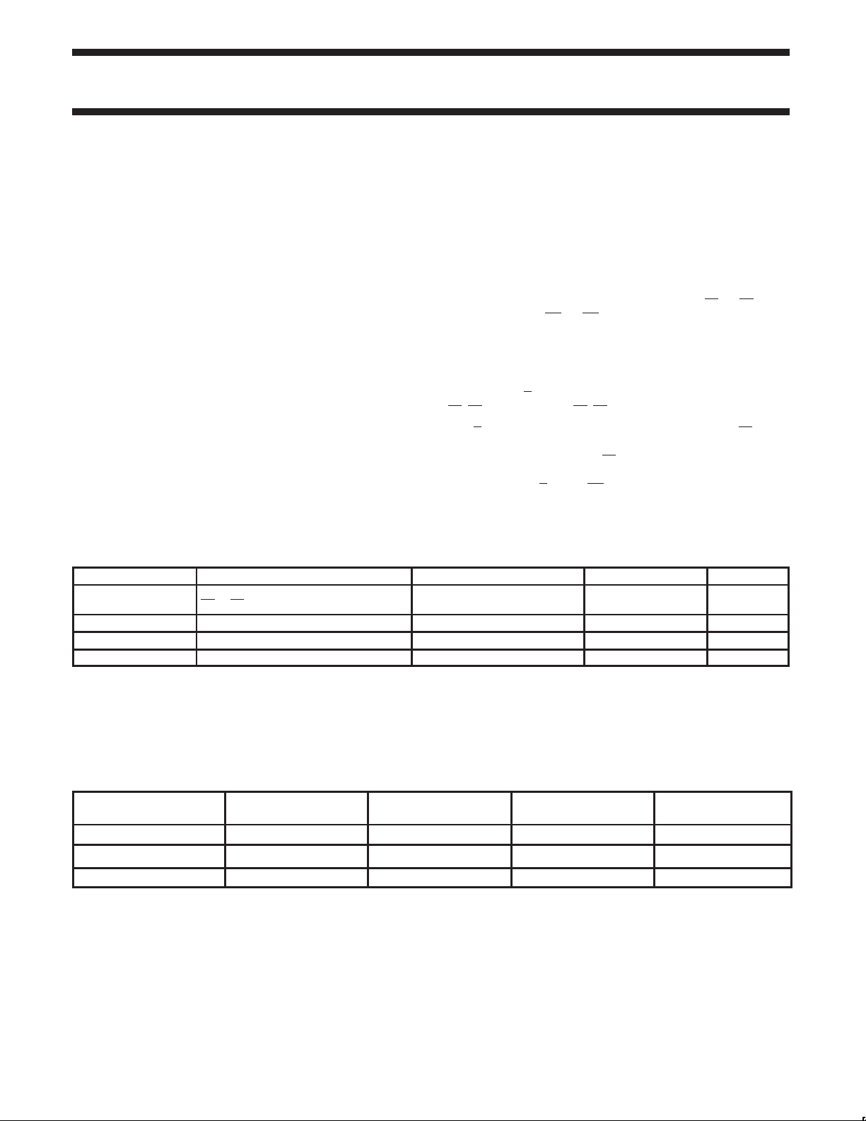
PIN DESCRIPTION
PIN NUMBER SYMBOL FUNCTION
1 LEBA
2 OEBA
3, 4, 5, 6,
7, 8, 9, 10
A0–A7 ‘A’ data inputs/outputs
11 EBA ‘B’ to ‘A’ enable input (active LOW)
12 GND Ground (0V)
22, 21, 20, 19,
18, 17, 16, 15
B0–B7 ‘B’ data inputs/outputs
13 OEAB
14 LEAB
23 EAB ‘A’ to ‘B’ enable input (active LOW)
24 VCC Positive supply voltage
‘B’ to ‘A’ latch enable input (active
LOW)
‘B’ to ‘A’ output enable input (active
LOW)
‘A’ to ‘B’ output enable input (active
LOW)
‘A’ to ‘B’ latch enable input (active
LOW)
PIN CONFIGURATION
1
BA
LE
2
OE
BA
3
A0
4
A1
5
A2
6
A3
7
A4
8
A5
9
A6
10
A7
11
EAB
12 13
GND
74LVC544A
24
V
CC
23
EBA
22
B0
21
B1
20
B2
19
B3
18
B4
17
B5
16
B6
15
B7
14
LEAB
OE
AB
SV00733
FUNCTION TABLE
INPUTS
OEXX EXX LEXX DATA
H X X X Z Disabled
X H X X Z Disabled
L
L
L
L
L
L
L L H X NC Hold
XX = AB for A-to-B direction, BA for B-to-A direction
H = HIGH voltage level
L = LOW voltage level
h = HIGH state must be present one set-up time before the LOW-to-HIGH transition of LE
l = LOW state must be present one set-up time before the LOW-to-HIGH transition of LEAB, LEBA, EAB, EBA
X = Don’t care
↑ = LOW–to–HIGH level transition
NC = No change
Z = High impedance OFF-state
↑
↑
L
L
L
L
L
L
↑
↑
L
L
h
l
h
l
H
L
Z
Z
L
H
L
H
AB, LEBA, EAB, EBA
Disabled + Latch
Latch + Display
Transparent
1998 Jul 29
3
 Loading...