

Philips 74lvc543a DATASHEETS

INTEGRATED CIRCUITS
74LVC543A
Octal D-type registered transceiver
(3-State)
Product specification
Supersedes data of 1998 Jul 31
IC24 Data Handbook
2000 Jun 21
Philips Semiconductors Product specification
Octal D-type registered transceiver (3-State)
FEA TURES
•5-volt tolerant inputs/outputs, for interfacing with 5-volt logic
•Supply voltage range of 1.2 V to 3.6 V
•Complies with JEDEC standard no. 8–1A
•CMOS low power consumption
•Direct interface with TTL levels
•8-bit octal transceiver with D-type latch
•Back-to-back registers for storage
•Separate controls for data flow in each direction
•3-State non-inverting outputs for bus oriented applications
•High impedance when V
QUICK REFERENCE DATA
GND = 0V; T
SYMBOL
t
PHL/tPLH
C
I
C
I/O
C
PD
NOTES:
is used to determine the dynamic power dissipation (PD in µW)
1. C
PD
P
= CPD x V
D
= input frequency in MHz; CL = output load capacity in pF;
f
i
f
= output frequency in MHz; VCC = supply voltage in V;
o
Σ (C
L
2. The condition is V
x V
amb
CC
= 25°C; Tr = T
Propagation delay
An to B
input capacitance 5.0 pF
input/output capacitance 10.0 pF
power dissipation capacitance per latch VCC = 3.3 V 27 pF
2
x fi +Σ (CL x V
CC
2
x f
o )
= 0 V
CC
≤ 2.5ns
f
PARAMETER CONDITIONS TYPICAL UNIT
n
2
x f
CC
= sum of the outputs
= GND to V
I
CC
where:
o )
DESCRIPTION
The 74LVC543A is a high-performance, low-power, low-voltage,
Si-gate CMOS device and superior to most advanced CMOS
compatible TTL families.
The 74LVC543A is an octal registered transceiver containing two
sets of D-type latches for temporary storage of the data flow in
either direction. Separate latch enable (LE
enable (OE
independent control of inputting and outputting in either direction of
the data flow.
The 74LVC543A contains eight D-type latches, with separate inputs
and controls for each set. For data flow from A to B, for example, the
A-to-B enable (E
A
0-A7
With E
input makes the A-to-B latches transparent; a subsequent
LOW–to-HIGH transition of the LEAB signal puts the A data into the
latches where it is stored and the B outputs no longer change with
the A inputs. With E
buffers are active and display the data present at the outputs of the
A latches
74LVC543A
, LEBA) and output
, OEBA) inputs are provided for each register to permit
AB
) input must be LOW in order to enter data from
or take data from B0-B7, as indicated in the function table.
AB
AB
LOW, a LOW signal on the A-to-B latch enable (LEAB)
and OEAB both low, the 3-state B output
AB
CL = 50 pF
VCC = 3.3 V
AB
3.3 ns
ORDERING INFORMATION
PACKAGES
24-Pin P lastic Small Outline (SO) –40°C to +85°C 74LVC543A D 74LVC543A D SOT137-1
24-Pin Plastic Shrink Small Outline (SSOP) Type II –40°C to +85°C 74LVC543A DB 74LVC543A DB SOT340-1
24-Pin Plastic Thin Shrink Small Outline (TSSOP) Type I –40°C to +85°C 74LVC543A PW 7LVC543APW DH SOT355-1
2000 Jun 21 853-1992 23942
TEMPERATURE
RANGE
2
OUTSIDE NORTH
AMERICA
NORTH AMERICA PKG DWG. #
Philips Semiconductors Product specification
74LVC543AOctal D-type registered transceiver (3-State)
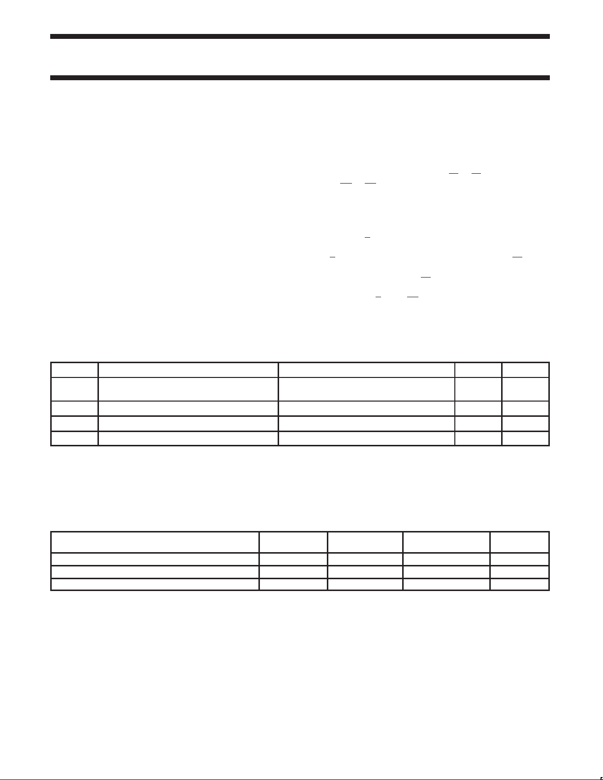
PIN CONFIGURATION
1
LE
BA
2
OE
BA
3
A0
4
A1
5
A2
6
A3
7
A4
8
A5
9
A6
10
A7
11
E
BA
12 13
GND
SW00212
24
V
CC
23
E
AB
22
B0
21
B1
20
B2
19
B3
18
B4
17
B5
16
B6
15
B7
14
LE
AB
OE
AB
PIN DESCRIPTION
PIN NUMBER SYMBOL FUNCTION
1 LE
2 OE
BA
BA
3,4,5,6, 7, 8, 9 10 A0 to A
11 E
BA
12 GND ground (0V)
22, 21, 20, 19,
18, 17, 16, 15
13 OE
14 LE
23 E
24 V
B0 to B
AB
AB
AB
CC
‘B’ to ‘A’ latch enable input
(active LOW)
‘B’ to ‘A’ output enable
input (active LOW)
‘A’ data inputs/outputs
7
‘B’ to ‘A’ enable input
(active LOW)
‘B’ data inputs/outputs
7
‘A’ to ‘B’ output enable
input (active LOW)
‘A’ to ‘B’ latch enable input
(active LOW)
‘A’ to ‘B’ enable input
(active LOW)
positive supply voltage
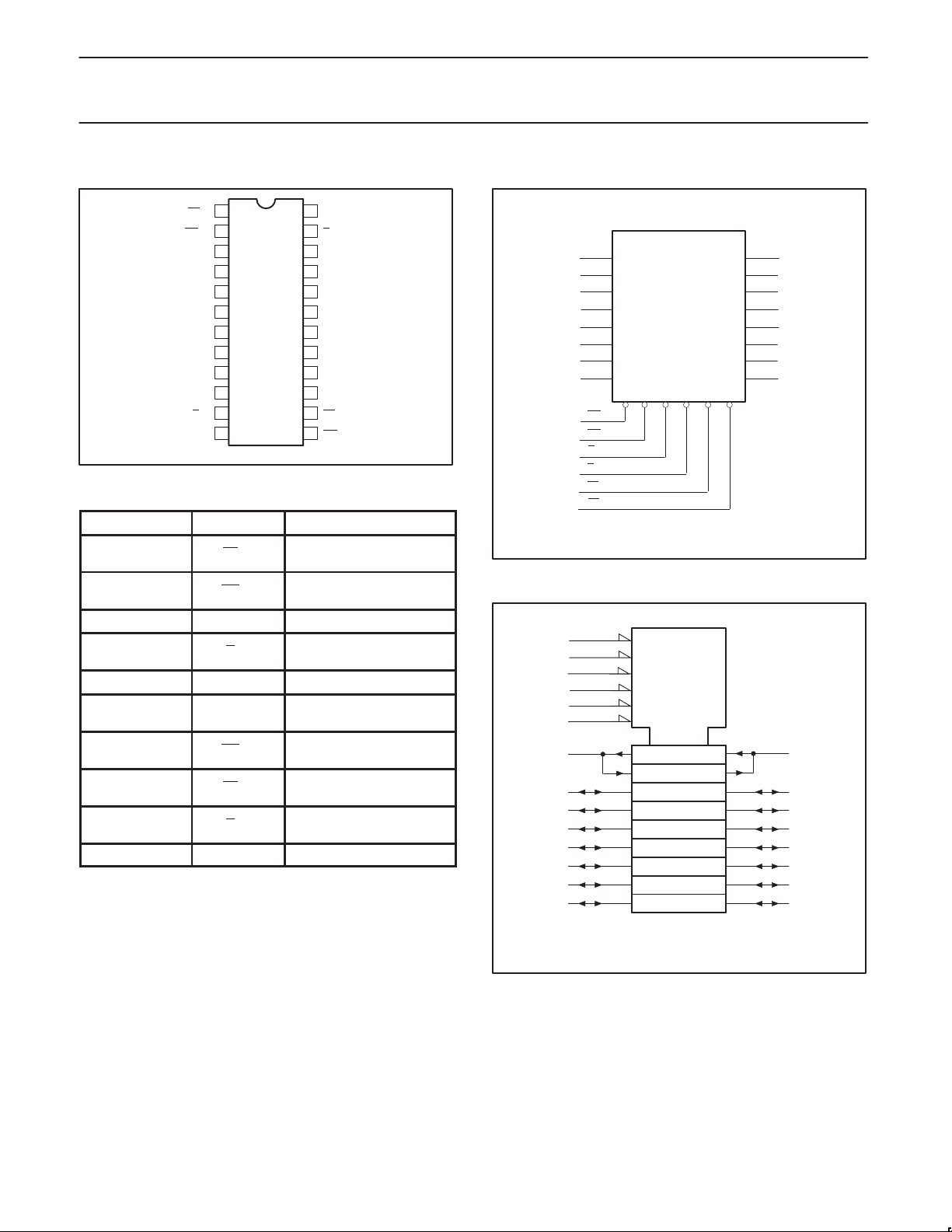
LOGIC SYMBOL
3
A0
4
A1
5
A2
6
A3
A4
7
A5
8
A6
9
10
A7
OE
2
BA
13
OE
AB
11
E
BA
E
23
AB
14
LE
AB
1
LE
BA
LOGIC SYMBOL (IEEE/IEC)
2
23
1
13
11
14
3
4
5
6
7
8
9
10
1EN3
G1
1C5
2EN4
G2
2C6
∇ 3
6D
5D
4 ∇
B0
B1
B2
B3
B4
B5
B6
B7
SW00213
22
21
20
19
18
17
16
15
22
21
20
19
18
17
16
15
2000 Jun 21
SW00214
3
Philips Semiconductors Product specification
OPERATING MODES
OUTPUTS
Disabled
XHXXZ
LLHXNC
74LVC543AOctal D-type registered transceiver (3-State)
LOGIC DIAGRAM
OE
BA
E
BA
LE
BA
OE
AB
E
AB
LE
AB
LE
D
B
A
n
LE
D
8 IDENTICAL
CHANNELS
n
TO 7 OTHER CHANNELS
FUNCTION TABLE
INPUTS
OE
XX
Disabled H X X X Z
Disabled + Latch
Latch + Display
Transparent
L
L
L
L
L
L
Hold
(do nothing)
NOTES:
XX = AB for A-to-B direction, BA for B-to-A direction
H = High voltage level
L = Low voltage level
h = High state must be present one setup time before the Low-to-High transition of LE
l = Low state must be present one setup time before the Low-to-High transition of LEAB, LEBA, EAB, E
X = Don’t care
↑ = Low-to-High level transition
NC = No change
Z = High impedance OFF state
E
XX
↑
↑
L
L
L
L
LE
XX
L
L
↑
↑
L
L
, LEBA, EAB, E
AB
BA
BA
SW00215
DATA
h
l
h
l
H
L
Z
Z
H
L
H
L
2000 Jun 21
4
 Loading...