

Philips 74LVC541APW, 74LVC541ADB, 74LVC541AD Datasheet
INTEGRATED CIRCUITS
74LVC541A
Octal buffer/line driver with 5-volt tolerant
inputs/outputs (3-State)
Product specification
Supercedes data of 1997 Oct 27
IC24 Data Handbook
1998 Jul 29
Philips Semiconductors Product specification
Octal buffer/line driver with 5-volt tolerant
inputs/outputs (3-State)
FEA TURES
•5-volt tolerant inputs/outputs, for interfacing with 5-volt logic
•Wide supply voltage range of 2.7V to 3.6V
•Complies with JEDEC standard no. 8-1A
•CMOS low power consumption
•Direct interface with TTL levels
•5 Volt tolerant inputs/outputs, for interfacing with 5 Volt logic
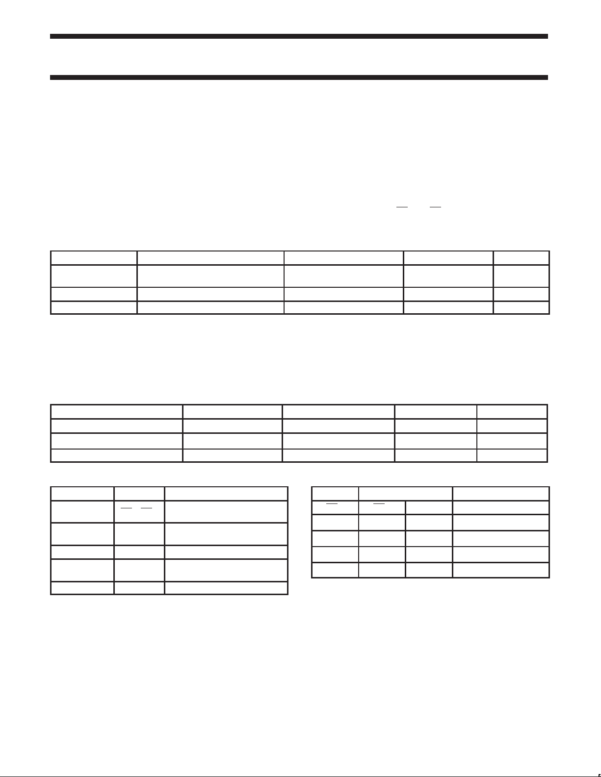
QUICK REFERENCE DATA
GND = 0 V; T
SYMBOL
t
NOTES:
is used to determine the dynamic power dissipation (PD in µW)
1. C
PD
P
= CPD × V
D
fi = input frequency in MHz; CL = output load capacitance in pF;
= output frequency in MHz; VCC = supply voltage in V;
f
o
(C
L
2. The condition is VI = GND to V
= 25°C; tr = tf ≤ 2.5 ns
amb
PHL/tPLH
C
I
C
PD
2
× fi (CL × V
CC
2
× V
× fo) = sum of the outputs.
CC
PARAMETER CONDITIONS TYPICAL UNIT
Propagation delay
An to Yn
Input capacitance 5.0 pF
Power dissipation capacitance per buffer Notes 1 and 2 20 pF
2
× fo) where:
CC
CC
CL = 50 pF;
VCC = 3.3 V
74L VC541A
DESCRIPTION
The 74LVC541A is a high performance, low-power, low-voltage
Si-gate CMOS device and superior to most advanced CMOS
compatible TTL families.
Inputs can be driven from either 3.3V or 5.0V devices. In 3-State
operation, outputs can handle 5V. This feature allows the use of
these devices as translators in a mixed 3.3V/5V environment.
The 74LVC541A is an octal non-inverting buffer/line driver with
5-volt tolerant inputs/outputs. The 3-State outputs are controlled by
the output enable inputs OE
1 and OE2.
3.3 ns
ORDERING INFORMATION
PACKAGES TEMPERATURE RANGE OUTSIDE NORTH AMERICA NORTH AMERICA PKG. DWG. #
20-Pin Plastic SO –40°C to +85°C 74LVC541A D 74LVC541A D SOT163-1
20-Pin Plastic SSOP Type II –40°C to +85°C 74LVC541A DB 74LVC541A DB SOT339-1
20-Pin Plastic TSSOP Type I –40°C to +85°C 74LVC541A PW 7LVC541APW DH SOT360-1
PIN DESCRIPTION
PIN NUMBER SYMBOL NAME AND FUNCTION
1, 19 OE1, OE2
2, 3, 4, 5,
6, 7, 8, 9
10 GND Ground (0 V)
18, 17, 16, 15,
14, 13, 12, 11
20 V
A0 to A7 Data inputs
Y0 to Y7 Bus outputs
CC
Output enable inputs
(active LOW)
Positive supply voltage
FUNCTION TABLE
INPUTS INPUTS OUTPUT
OE1 OE2 An Yn
L L L L
L L H H
X H X Z
H X X Z
H = HIGH voltage level
L = LOW voltage level
X = don’t care
Z = high impedance OFF-state
1998 Jul 29 853-2103 19803
2
Philips Semiconductors Product specification
Octal buffer/line driver with 5-volt tolerant
inputs/outputs (3-State)
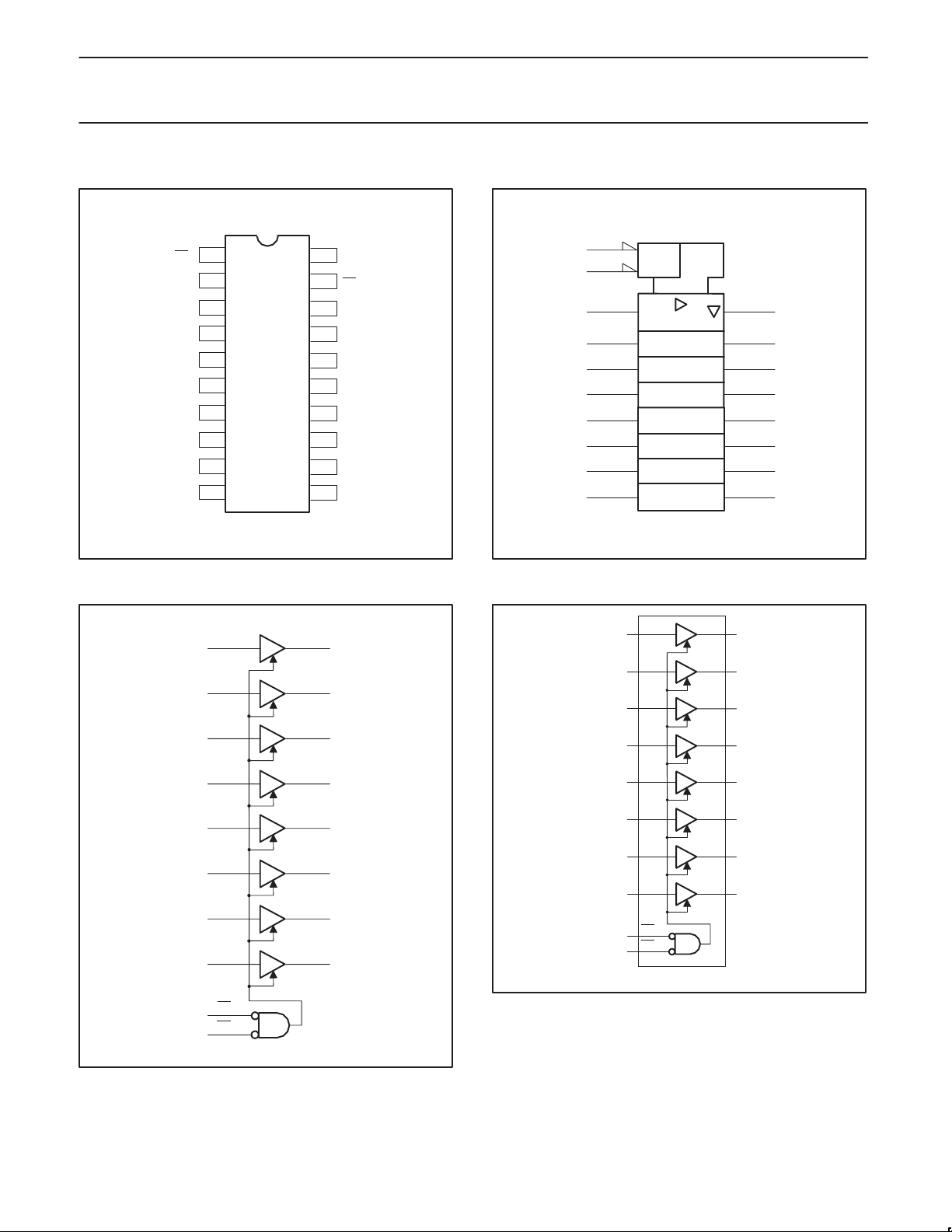
PIN CONFIGURATION
1
OE
GND
1
A
2
0
3
A
1
4
A
2
5
A
3
6
A
4
A
7
5
8
A
6
9
A
7
10
20
V
CC
19
OE
2
18
Y
0
Y
17
1
16
Y
2
15
Y
3
14
Y
4
13
Y
5
Y
12
6
Y
11
7
LOGIC SYMBOL (IEEE/IEC)
1
19
2
3
4
5
6
7
8
9
&
74LVC541A
EN
18
17
16
15
14
13
12
11
LOGIC SYMBOL
SV00680
SV00682
FUNCTIONAL DIAGRAM
A
0
A
0
2
A
1
3
A
2
4
A
3
5
A
4
6
A
5
7
A
6
8
A
7
9
OE
1
1
OE
2
19
Y
0
18
Y
1
17
Y
2
16
Y
3
15
Y
4
14
Y
5
13
Y
6
12
Y
7
11
2
A
1
3
A
2
4
A
3
5
A
4
6
A
5
7
A
6
8
A
7
9
OE
1
1
OE
2
19
Y
0
Y
1
Y
2
Y
3
Y
4
Y
5
Y
6
Y
7
SV00683
18
17
16
15
14
13
12
11
1998 Jul 29
SV00681
3
 Loading...