

Philips 74LVC377PW, 74LVC377DB, 74LVC377D Datasheet
INTEGRATED CIRCUITS
74LVC377
Octal D-type flip-flop with data enable;
positive-edge trigger
Product specification
Supersedes data of 1996 Jun 06
IC24 Data Handbook
1998 Jul 29

Philips Semiconductors Product specification
f
Maximum clock frequency
230
MHz
Octal D-type flip-flop with data enable;
positive-edge trigger
FEATURES
•Wide supply voltage range of 1.2V to 3.6V
•Conforms to JEDEC standard 8-1A
•Inputs accept voltages up to 5.5V
•CMOS low power consumption
•Direct interface with TTL levels
•Output drive capability 50Ω transmission lines @ 85°C
QUICK REFERENCE DATA
GND = 0V; T
SYMBOL
t
PHL/tPLH
max
C
I
C
PD
NOTES:
is used to determine the dynamic power dissipation (PD in µW)
1C
PD
= CPD V
P
D
= input frequency in MHz; CL = output load capacity in pF;
f
i
f
= output frequency in MHz; VCC = supply voltage in V;
o
(C
= 25°C; tr =tf 2.5 ns
amb
CC
2
V
L
fo) = sum of the outputs.
CC
PARAMETER CONDITIONS TYPICAL UNIT
Propagation delay
CP to Qn;
Input capacitance 5.0 pF
Power dissipation
capacitance per flip-flop
2
x fi (CL V
2
fo) where:
CC
74L VC377
DESCRIPTION
The 74LVC377 is a low-voltage Si-gate CMOS device, superior to
most advanced CMOS compatible TTL families.
The 74LVC377 has eight edge-triggered , D-type flip-flops with
individual D inputs and Q outputs. A common clock (CP) input loads
all flip-flops simultaneously when the data enable E
state of each D input, one set-up time before the LOW-to-HIGH
clock transition, is transferred to the corresponding output (Qn) of
the flip-flop. The E
input must be stable only one set-up time prior to
the LOW-to-HIGH transition for predictable operation.
CL = 50pF
VCC = 3.3V
VI = GND to V
CC
1
6.0 ns
22 pF
is LOW. The
ORDERING INFORMATION
PACKAGES TEMPERATURE RANGE OUTSIDE NORTH AMERICA NORTH AMERICA DWG NUMBER
20-Pin Plastic SO –40°C to +85°C 74LVC377 D 74LVC377 D SOT163-1
20-Pin Plastic SSOP Type II –40°C to +85°C 74LVC377 DB 74LVC377 DB SOT339-1
20-Pin Plastic TSSOP Type I –40°C to +85°C 74LVC377 PW 74LVC377PW DH SOT360-1
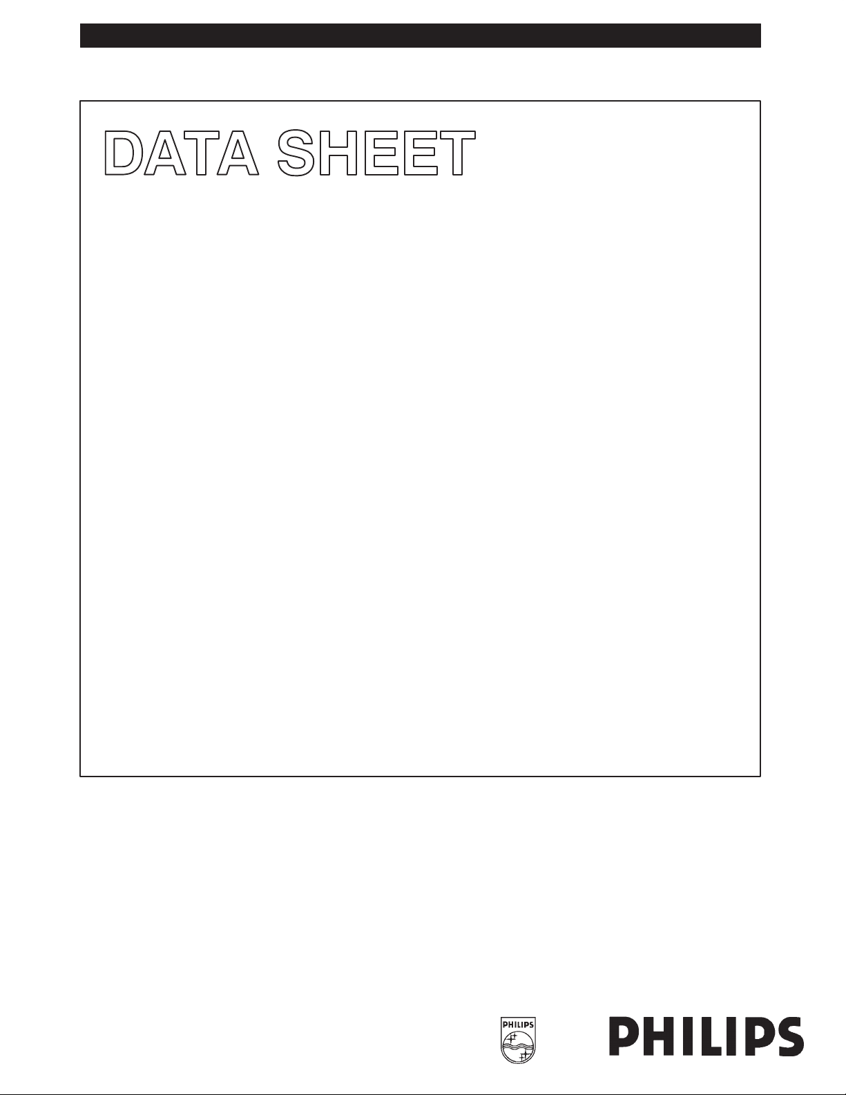
PIN CONFIGURATION
1
2
Q0
3
D0
4
D1
5
Q1
6
Q2
7
D2
8
D3
9
Q3
GND
20E
19
18
17
16
15
14
13
12
1110
SY00058
V
Q7
D7
D6
Q6
Q5
D5
D4
Q4
CP
CC
PIN DESCRIPTION
PIN
NUMBER
1 E Data enable input (active LOW)
2, 5, 6,
9, 12, 15,
16, 19
3, 4, 7,
8, 13, 14,
17, 18
10 GND Ground (0V)
11 CP
20 V
SYMBOL FUNCTION
Q0 – Q7 Flip-flop outputs
D0 – D7 Data inputs
Clock input (LOW-to-HIGH,
edge-triggered)
CC
Positive power supply
1998 Jul 29
2
Philips Semiconductors Product specification
SYMBOL
PARAMETER
CONDITIONS
UNIT
Octal D-type flip-flop with data enable;
positive-edge trigger
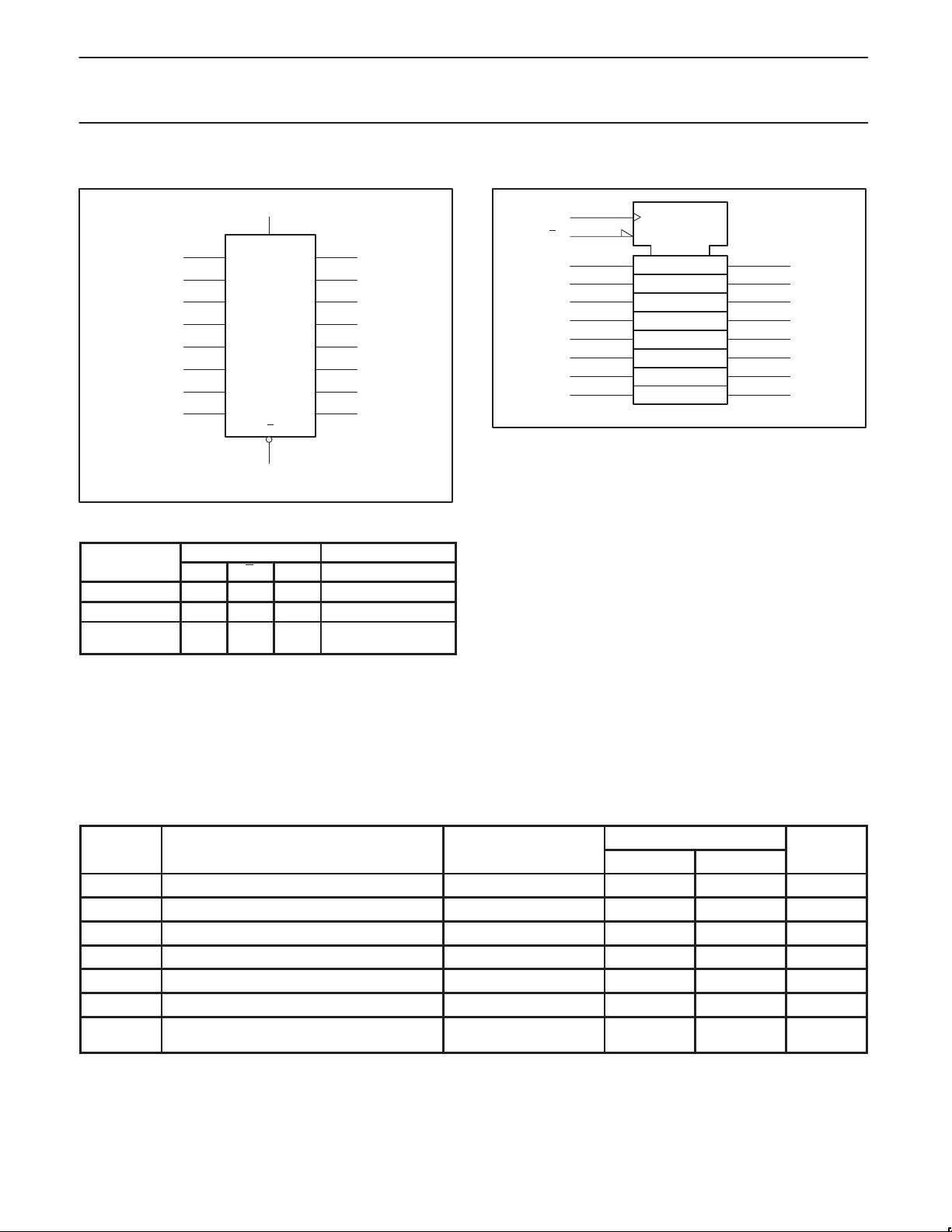
LOGIC SYMBOL
11
3
4
7
8
13
14
17
18
FUNCTION TABLE
OPERATING
MODES
Load ‘1’ l h H
Load ‘0’ l l L
hold
(do nothing)
H = HIGH voltage level
h = HIGH voltage level one set-up time
prior to the LOW-to-HIGH CP transition
L = LOW voltage level
I = LOW voltage level one set-up time
prior to the LOW-to-HIGH CP transition
= LOW-to-HIGH transition
X = Don’t care
CP E Dn Q
X
CP
D0
D1
D2
D3
D4
D5
D6
D7
Q0
Q1
Q2
Q3
Q4
Q5
Q6
Q7
E
1
2
5
6
9
12
15
16
19
SY00059
INPUTS OUTPUT
n
h
H
X
X
no change
no change
LOGIC SYMBOL (IEEE/IEC)
CP
E
D0
D1
D2
D3
D4
D5
D6
11
1
3
4
7
8
13
14
17
18
1C2
G1
2D
74LVC377
2
Q0
5
Q1
6
Q2
9
Q3
12
Q4
15
Q5
16
Q6
19
Q7D7
SY00060
RECOMMENDED OPERA TING CONDITIONS
V
CC
V
CC
V
V
I/O
V
T
amb
tr, t
1998 Jul 29
DC supply voltage (for max. speed performance) 2.7 3.6 V
DC supply voltage (for low-voltage applications) 1.2 3.6 V
DC Input voltage range 0 5.5 V
I
DC Input voltage range for I/Os 0 V
DC output voltage range 0 V
O
Operating free-air temperature range –40 +85 °C
Input rise and fall times
f
VCC = 1.2 to 2.7V
VCC = 2.7 to 3.6V
3
LIMITS
MIN MAX
CC
CC
0
0
20
10
V
V
ns/V
 Loading...