

Philips 74LVC2952APW, 74LVC2952ADB, 74LVC2952AD Datasheet
INTEGRATED CIRCUITS
74LVC2952A
Octal registered tranceiver with 5-volt
tolerant inputs/ouputs (3-State)
Product specification 1998 Jul 29
Philips Semiconductors Product specification
Octal registered tranceiver with 5-volt tolerant
inputs/ouputs (3-State)
FEA TURES
•5-volt tolerant inputs/outputs, for interfacing with 5-volt logic
•Wide supply voltage range of 1.2 V to 3.6 V
•In accordance with the JEDEC standard no. 8-1 A
•Inputs accept voltages up to 5.5 V
•CMOS low power consumption
•Flow-through pin-out architecture
•3-State outputs
•Direct interface with TTL levels
•Integrated 30 damping resistor
QUICK REFERENCE DATA
GND = 0 V; T
= 25°C; tr =t
amb
SYMBOL
t
PHL/tPLH
f
max
C
I
C
I/O
C
PD
Propagation delay
CPnn to An, B
Maximum clock frequency 150 MHz
Input capacitance 5 pF
Input/output capacitance 10 pF
Power dissipation capacitance per buffer VCC = 3.3V
NOTE:
1C
is used to determine the dynamic power dissipation (PD in µW)
PD
P
= CPD × V
D
2
× fi (CL × V
CC
fi = input frequency in MHz; CL = output load capacity in pF;
f
= output frequency in MHz; VCC = supply voltage in V;
o
(C
2
× V
× fo) = sum o f t h e o u t p u t s .
L
CC
≤ 2.5 ns
f
PARAMETER CONDITIONS TYPICAL UNIT
n
2
× fo) where:
CC
CL = 50 pF;
VCC = 3.3 V
DESCRIPTION
The 74LVC2952A is a low-power, low-voltage, Si-gate CMOS device
and superior to most advanced CMOS compatible TTL families. The
74LVC2952A is an octal non-inverting registered transceiver. Two 8-bit
back to back registers store data flowing in both directions between two
bidirectional busses. Data applied to the inputs is entered and stored on
the rising edge of the clock (CPnn) provided that the clock enable CE
is LOW. The data is then present at the 3-State output buffers, but is
only accessible when the output enable input (OE
from A inputs to B outputs is the same as for B inputs to A outputs. The
74LVC2952A is identical to the 74LVC2953A but has non-inverting
outputs.
1
74L VC2952A
) is LOW. Data flow
nn
4.3 ns
31 pF
)
nn
ORDERING INFORMATION
PACKAGES TEMPERATURE RANGE OUTSIDE NORTH AMERICA NORTH AMERICA PKG. DWG. #
24-Pin Plastic SO –40°C to +125°C 74LVC2952A D 74LVC2952A D SOT137-1
24-Pin Plastic SSOP Type II –40°C to +125°C 74LVC2952A DB 74LVC2952A DB SOT340-1
24-Pin Plastic TSSOP Type I –40°C to +125°C 74LVC2952A PW 74LVC2952APW DH SOT355-1
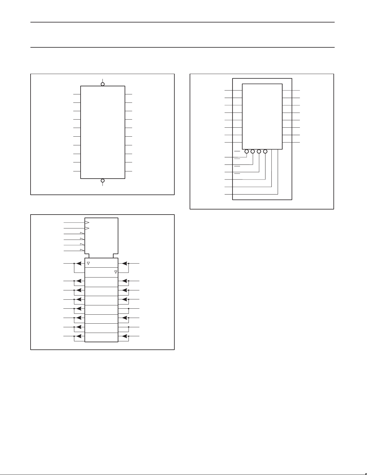
PIN CONFIGURATION
B
1
7
B
2
6
B
3
5
B
4
4
B
5
3
B
6
2
B
7
1
B
8
0
OE
9
AB
CP
10
AB
11
CE
AB
12
GND
24
V
CC
A
23
7
A
22
6
A
21
5
20
A
4
19
A
3
18
A
2
A
17
1
16
A
0
15
OE
BA
14
CP
BA
13
CE
BA
SV01716
PIN DESCRIPTION
PIN NUMBER SYMBOL FUNCTION
8, 7, 6, 5, 4, 3, 2, 1, B0 to B
12 GND Ground (0 V)
9, 15 OEAB,OE
10, 14 CPAB, CPBAClock inputs
11, 13, CEAB, CEBAClock enable inputs
16, 17, 18, 19, 20,
21, 22, 23
24 V
A0 to A
CC
B data inputs/outputs
7
Output enable inputs
BA
(active LOW)
A data inputs/outputs
7
Positive supply voltage
1998 Jul 29 853-1993 19803
2
Philips Semiconductors Product specification
Octal registered tranceiver with 5-volt tolerant
inputs/ouputs (3-State)
LOGIC SYMBOL (IEEE/IEC)
9
OE
CP
10
CE
11
A
16
A
17
A
18
A
19
A
20
21
A
A
22
A
23
AB
OE
CP
CE
BA
15
AB
AB
0
1
2
3
4
5
6
7
BA
BA
B
0
B
1
B
2
B
3
B
4
B
5
B
6
B
7
SV01717
14
13
8
7
6
5
4
3
2
1
FUNCTIONAL DIAGRAM
16
A
0
A
17
1
A
18
2
A
19
3
A
20
4
A
21
5
A
22
6
A
23
7
9
OE
AB
15
OE
BA
11
CE
AB
13
CE
BA
10
CP
AB
14
CP
BA
74LVC2952A
B
8
0
7
B
1
6
B
2
5
B
3
4
B
4
3
B
5
2
B
6
1
B
7
LOGIC SYMBOL
14
10
13
11
15
9
16
17
18
19
20
21
22
23
G1
G2
EN3
EN4
6D
1 C5
2 C6
3
SV01719
1
5D
4
1
8
7
6
5
4
3
2
1
SV01718
1998 Jul 29
3
Philips Semiconductors Product specification
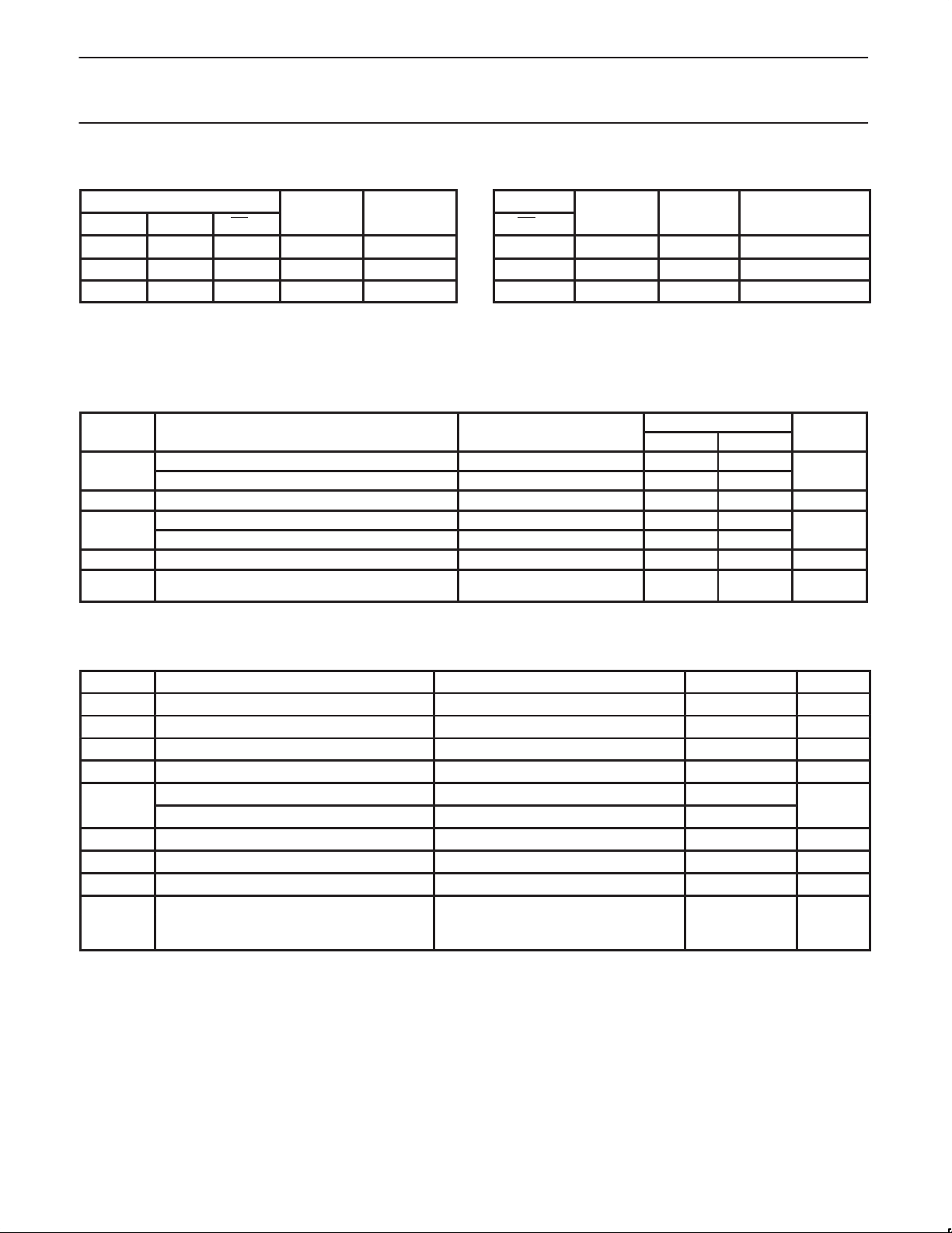
n n
OPERATING MODE
SYMBOL
PARAMETER
CONDITIONS
UNIT
V
V
V
V
V
V
mW
Octal registered tranceiver with 5-volt tolerant
inputs/ouputs (3-State)
FUNCTION TABLE for register An or B
INPUTS
An or B
CP
n
nn
CE
X X H NC Hold data
L ↑ L L Load data
H ↑ L H Load data
NOTES:
H = HIGH voltage level
L = LOW voltage level
X = don’t care
INTERNAL OPERATING
nn
RECOMMENDED OPERATING CONDITIONS
DC supply voltage (for max. speed performance) 2.7 3.6
DC supply voltage (for low-voltage applications) 1.2 3.6
DC input voltage range 0 5.5 V
I
DC output voltage range; output HIGH or LOW state 0 V
DC input voltage range; output 3-State 0 5.5
Operating free-air temperature range –40 +85 °C
Input rise and fall times
f
T
CC
V
I/O
amb
tr, t
n
Q MODE
74LVC2952A
FUNCTION TABLE for output enable
INPUTS
OE
nn
H X Z Disable outputs
L L L Enable outputs
L H H Enable outputs
Z = high impedance OFF-state
↑ = Low-to-High transition
NC = no change
VCC = 1.2 to 2.7V
VCC = 2.7 to 3.6V
INTERNAL An or B
Q
OUTPUTS
LIMITS
MIN MAX
0
0
n
CC
20
10
ns/V
ABSOLUTE MAXIMUM RATINGS
1
In accordance with the Absolute Maximum Rating System (IEC 134).
Voltages are referenced to GND (ground = 0 V).
SYMBOL
V
CC
I
IK
V
I
I
OK
DC supply voltage –0.5 to +6.5 V
DC input diode current VIt 0 –50 mA
DC input voltage Note 2 –0.5 to +6.5 V
DC output diode current V
PARAMETER CONDITIONS RATING UNIT
uVCC or VO t 0 "50 mA
O
DC output voltage; output HIGH or LOW Note 2 –0.5 to VCC +0.5
I
GND
I/O
I
O
T
stg
DC output voltage; output 3-State Note 2 –0.5 to 6.5
DC output source or sink current VO = 0 to V
, I
DC VCC or GND current "100 mA
CC
CC
"50 mA
Storage temperature range –65 to +150 °C
Power dissipation per package
P
TOT
– plastic mini-pack (SO) above +70°C derate linearly with 8 mW/K 500
– plastic shrink mini-pack (SSOP and TSSOP) above +60°C derate linearly with 5.5 mW/K 500
NOTES:
1 Stresses beyond those listed may cause permanent damage to the device. These are stress ratings only and functional operation of the
device at these or any other conditions beyond those indicated under “recommended operating conditions” is not implied. Exposure to
absolute-maximum-rated conditions for extended periods may affect device reliability .
2 The input and output voltage ratings may be exceeded if the input and output current ratings are observed.
1998 Jul 29
4
 Loading...