

Philips 74LVC273PW, 74LVC273DB, 74LVC273D Datasheet
INTEGRATED CIRCUITS
74LVC273
Octal D-type flip-flop with reset;
positive-edge trigger
Product specification
Supersedes data of 1996 Jun 06
IC24 Data Handbook
1998 May 20

Philips Semiconductors Product specification
f
Maximum clock frequency
230
MHz
74L VC273Octal D-type flip-flop with reset; positive-edge trigger
FEA TURES
•Wide supply voltage range of 1.2V to 3.6V
•Conforms to JEDEC standard 8-1A
•Inputs accept voltages up to 5.5V
•CMOS low power consumption
•Direct interface with TTL levels
•Output drive capability 50Ω transmission lines @ 85°C
QUICK REFERENCE DATA
GND = 0V; T
SYMBOL
t
PHL/tPLH
max
C
I
C
PD
NOTE:
is used to determine the dynamic power dissipation (PD in µW)
1C
PD
= CPD V
P
D
= input frequency in MHz; CL = output load capacity in pF;
f
i
f
= output frequency in MHz; VCC = supply voltage in V;
o
(C
= 25°C; tr =tf 2.5 ns
amb
CC
2
V
L
fo) = sum of the outputs.
CC
PARAMETER CONDITIONS TYPICAL UNIT
Propagation delay
CP to Qn;
to Q
MR
n
Input capacitance 5.0 pF
Power dissipation
capacitance per flip-flop
2
x fi (CL V
2
fo) where:
CC
DESCRIPTION
The 74LVC273 is a low-voltage Si-gate CMOS device, superior to
most advanced CMOS compatible TTL families.
The 74LVC273 has eight edge-triggered , D-type flip-flops with
individual D inputs and Q outputs. The common clock (CP) and
master reset (MR
simultaneously . The state of each D input, one set-up time before
the LOW-to-HIGH clock transition, is transferred to the
corresponding output (Qn) of the flip-flop.
All outputs will be forced LOW independently of clock or data inputs
by a LOW voltage level on the MR
The device is useful for applications where the true output only is
required and the clock and master reset are common to all storage
elements.
CL = 50pF
VCC = 3.3V
VI = GND to V
CC
) inputs load and reset (clear) all flip-flops
input.
6.0
6.0
1
22 pF
ns
ORDERING INFORMATION
PACKAGES TEMPERATURE RANGE OUTSIDE NORTH AMERICA NORTH AMERICA DWG NUMBER
20-Pin Plastic SO –40°C to +85°C 74LVC273 D 74LVC273 D SOT163-1
20-Pin Plastic SSOP Type II –40°C to +85°C 74LVC273 DB 74LVC273 DB SOT339-1
20-Pin Plastic TSSOP Type I –40°C to +85°C 74LVC273 PW 74LVC273PW DH SOT360-1
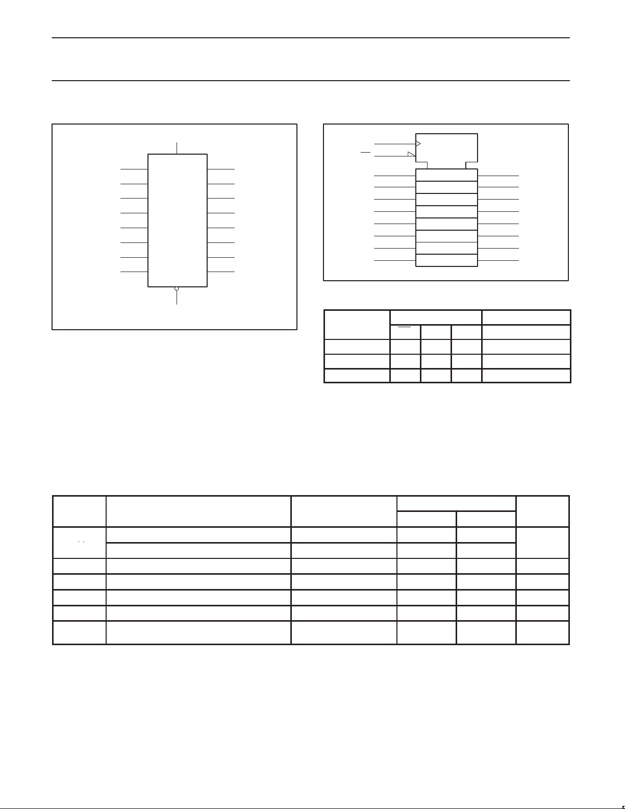
PIN CONFIGURATION
1
2
Q0
3
D0
4
D1
5
Q1
6
Q2
7
D2
8
D3
9
Q3
GND
20MR
19
18
17
16
15
14
13
12
1110
SY00051
V
Q7
D7
D6
Q6
Q5
D5
D4
Q4
CP
CC
PIN DESCRIPTION
PIN
NUMBER
1 MR Master reset input (active LOW)
2, 5, 6,
9, 12, 15,
16, 19
3, 4, 7,
8, 13, 14,
17, 18
10 GND Ground (0V)
11 CP
20 V
SYMBOL FUNCTION
Q0 – Q7 Flip-flop outputs
D0 – D7 Data inputs
Clock input (LOW-to-HIGH,
edge-triggered)
CC
Positive power supply
1998 May 20 853-2064 19419
2
Philips Semiconductors Product specification
SYMBOL
PARAMETER
CONDITIONS
UNIT
V
V
74LVC273Octal D-type flip-flop with reset; positive-edge trigger
LOGIC SYMBOL
3
4
7
8
13
14
17
18
IEEE/IEC LOGIC SYMBOL
11
CP
D0
D1
D2
D3
D4
D5
D6
D7
MR
Q0
Q1
Q2
Q3
Q4
Q5
Q6
Q7
2
5
6
9
12
15
16
19
CP
MR
D0
D1
D2
D3
D4
D5
D6
11
1
3
4
7
8
13
14
17
18
C1
R
2
1D
5
6
9
12
15
16
19
SY00050
Q0
Q1
Q2
Q3
Q4
Q5
Q6
Q7D7
FUNCTION TABLE
1
SY00052
OPERATING
MODES
Reset (clear) L X X L
Load ‘1’ H h H
Load ‘0’ H I L
H = HIGH voltage level
h = HIGH voltage level one set-up time prior to the
HIGH-to-LOW CP transition
L = LOW voltage level
I = LOW voltage level one set-up time prior to the
HIGH-to-LOW CP transition
= LOW-to-HIGH transition
X = Don’t care
INPUTS OUTPUT
MR CP Dn Q0 – Q7
RECOMMENDED OPERATING CONDITIONS
DC supply voltage (for max. speed performance) 2.7 3.6
DC supply voltage (for low-voltage applications) 1.2 3.6
DC Input voltage range 0 5.5 V
I
DC Input voltage range for I/Os 0 V
DC output voltage range 0 V
O
Operating free-air temperature range –40 +85 °C
Input rise and fall times
f
T
V
tr, t
CC
V
I/O
V
amb
VCC = 1.2 to 2.7V
VCC = 2.7 to 3.6V
LIMITS
MIN MAX
CC
CC
0
0
20
10
V
V
ns/V
1998 May 20
3
 Loading...