

Philips 74lvc257a DATASHEETS
INTEGRATED CIRCUITS
74LVC257A
Quad 2-input multiplexer with 5 Volt
tolerant inputs/outputs (3-State)
Product specification
Superceded data of 1997 Sep 26
IC24 Data Handbook
1998 Jul 29
Philips Semiconductors Product specification
Quad 2-input multiplexer with 5 Volt tolerant
inputs/outputs (3-State)
FEA TURES
•Wide supply voltage range of 1.2 to 3.6 V
•In accordance with JEDEC standard no. 8-1A
•CMOS lower power consumption
•Direct interface with TTL levels
•Output drive capability 50 transmission lines at 85°C
•5 Volt tolerant inputs/outputs, for interfacing with 5 Volt logic
QUICK REFERENCE DATA
GND = 0 V; T
= 25°C; tr =t
amb
SYMBOL
Propagation delay
t
PHL/tPLH
C
I
C
PD
nl0, nl1 to nY
S to nY
Input capacitance 5.0 pF
Power dissipation capacitance per channel VI = GND to V
NOTE:
is used to determine the dynamic power dissipation (PD in µW)
1. C
PD
P
= CPD × V
D
2
× fi (CL × V
CC
fi = input frequency in MHz; CL = output load capacitance in pF;
= output frequency in MHz; VCC = supply voltage in V;
f
o
(C
L
2
× V
× fo) = sum of the outputs.
CC
≤ 2.5 ns
f
PARAMETER CONDITIONS TYPICAL UNIT
2
× fo) where:
CC
CL = 50 pF;
VCC = 3.3 V
DESCRIPTION
The 74LVC257A is a high-performance, low-power, low-voltage,
Si-gate CMOS device and superior to most advanced CMOS
compatible TTL families.
Inputs can be driven from either 3.3V or 5.0V devices. In 3-State
operation, outputs can handle 5V. This feature allows the use of
these devices as translators in a mixed 3.3V/5V environment.
The 74LVC257A is a quad 2-input multiplexer with 3-state outputs,
which select 4 bits of data from two sources and are controlled by a
common data select input (S). The data inputs from source 0 (1l
4l
) are selected when input S is LOW and the data inputs from
0
source 1 (1l
outputs (1Y to 4Y) in true (non-inverting) form from the selected inputs.
The 74LVC257A is the logic implementation of a 4-pole, 2-position
switch, where the position of the switch is determined by the logic
levels applied to S. The outputs are forced to a high impedance
OFF-state when OE
1
CC
74L VC257A
to
0
to 4l1) are selected when S in HIGH. Data appears at the
1
is HIGH.
3.9
3.5
30 pF
ns
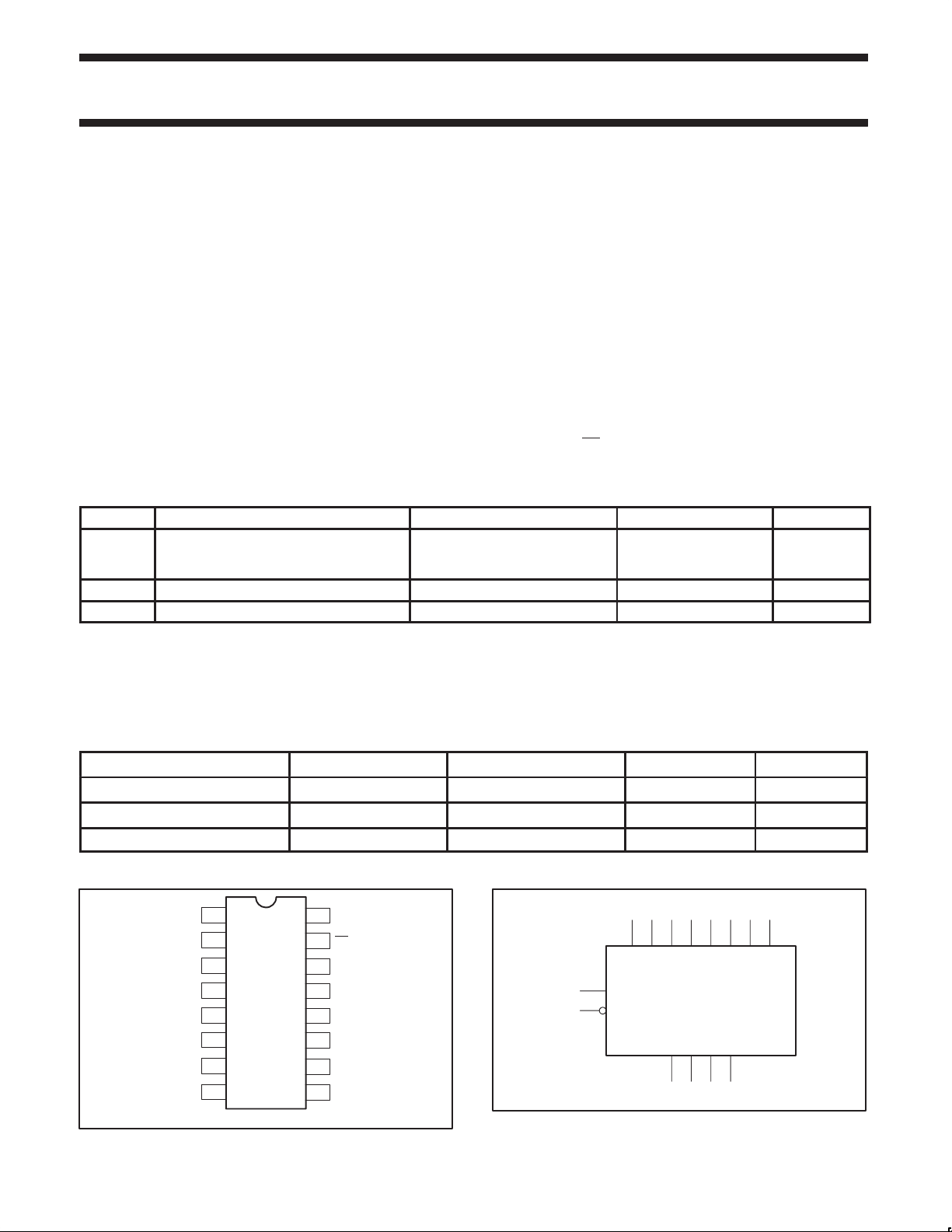
ORDERING INFORMATION
PACKAGES TEMPERATURE RANGE OUTSIDE NORTH AMERICA NORTH AMERICA PKG. DWG. #
16-Pin Plastic SO –40°C to +85°C 74LVC257A D 74LVC257A D SOT109-1
16-Pin Plastic SSOP Type II –40°C to +85°C 74LVC257A DB 74LVC257A DB SOT338-1
16-Pin Plastic TSSOP Type I –40°C to +85°C 74LVC257A PW 74LVC257APW DH SOT403-1
PIN CONFIGURATION
1
S
2
1I
0
3
1I
1
4
IY
5
2l
0
6
2l
1
7
2Y
8
GND
1998 Jul 29 853-2101 19802
16
15
14
13
12
11
10
9
SV00636
V
OE
4l
4l
4Y
3l
3l
3Y
CC
0
1
0
1
LOGIC SYMBOL
2
2
35
6
10
1411
13
1I
2I
3I
11I2I
0
0
1
1
15
S
OE
1Y
2Y
4
7
4I
3I
0
3Y
9
4I
0
1
1
4Y
12
SV00637
Philips Semiconductors Product specification
Quad 2-input multiplexer with 5 Volt tolerant
inputs/outputs (3-State)
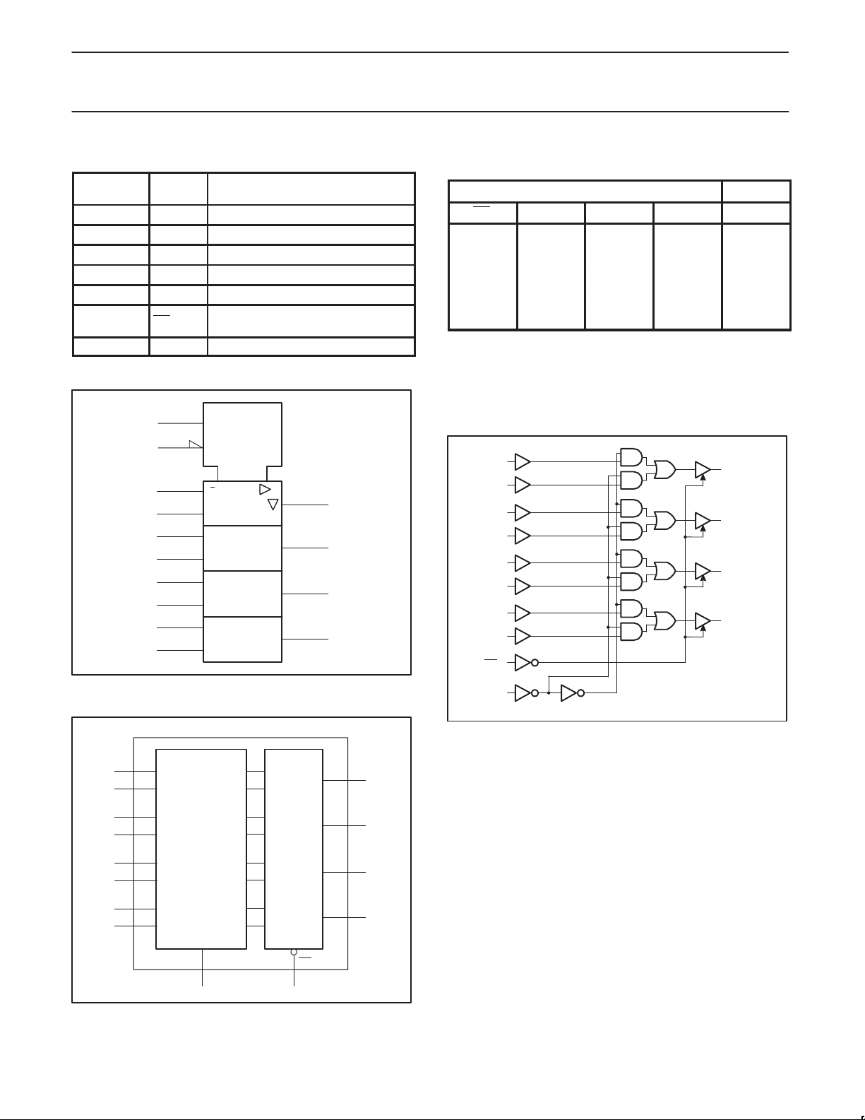
PIN DESCRIPTION
PIN
NUMBER
1 S Common data select input
2, 5, 11, 14 1l0 to 4l0Data inputs from source 0
3, 6, 10, 13 1l1 to 4l1Data outputs from source 1
4, 7, 9, 12 1Y to 4Y 3-State multiplexer outputs
8 GND Ground (0 V)
15 OE
16 V
LOGIC SYMBOL (IEEE/IEC)
SYMBOL FUNCTION
3-State output enable input (active
LOW)
CC
1
15
2
3
5
6
11
10
14
13
Positive supply voltage
G1
EN
MUX
1
1
SV00638
4
7
9
12
74LVC257A
FUNCTION TABLE
INPUTS OUTPUTS
OE S nl
0
H X X X Z
L H X L L
L H X H H
L L L X L
L L H X H
NOTES:
H = HIGH voltage level
L = LOW voltage level
X = don’t care
Z = high impedance OFF-state
LOGIC DIAGRAM
1I
1
1I0
2I
1
2I
0
3I
1
3I
0
4I
1
4I
0
OE
nl
1
nY
1Y
2Y
3Y
4Y
FUNCTIONAL DIAGRAM
2
1I
0
3
1I
1
5
2I
0
6
2I
1
11
10
14
13
1998 Jul 29
3I
3I
4I
4I
SELECTOR
0
1
0
1
S
115
3–STATE
MULTIPLEXER
OUTPUTS
OE
1Y
2Y
3Y
4Y
SV00639
S
SV00640
4
7
9
12
3
 Loading...