

Philips 74LVC245 Service Manual
Philips Semiconductors Product Specification
Octal bus transceiver with direction pin; 3-state 74LVC245
FEATURES
• Wide supply voltage range of
1.2 V to 3.6 V
• In accordance with the JEDEC
standard no. 8-1A.
• Inputs accept voltages upto
5.5 V
• Direct interface with TTL levels
• CMOS low power consumption
• Output drive capability 50 Ω
transmission lines @85°C
DESCRIPTION
The 74LVC245 is a
high-performance, low-power,
low-voltage, Si-gate CMOS device
and superior to most advanced
CMOS compatible TTL families.
The 74LVC245 is an octal
transceiver featuring non-inverting
3-state bus compatible outputs in
both send and receive directions.
The ’245’ features an output enable
(OE) input for easy cascading and a
send/receive (DIR) input for direction
control. OE controls the outputs so
that the buses are effectively
isolated.
The ’245’ is identical to the ’640’ but
has true (non-inverting) outputs.
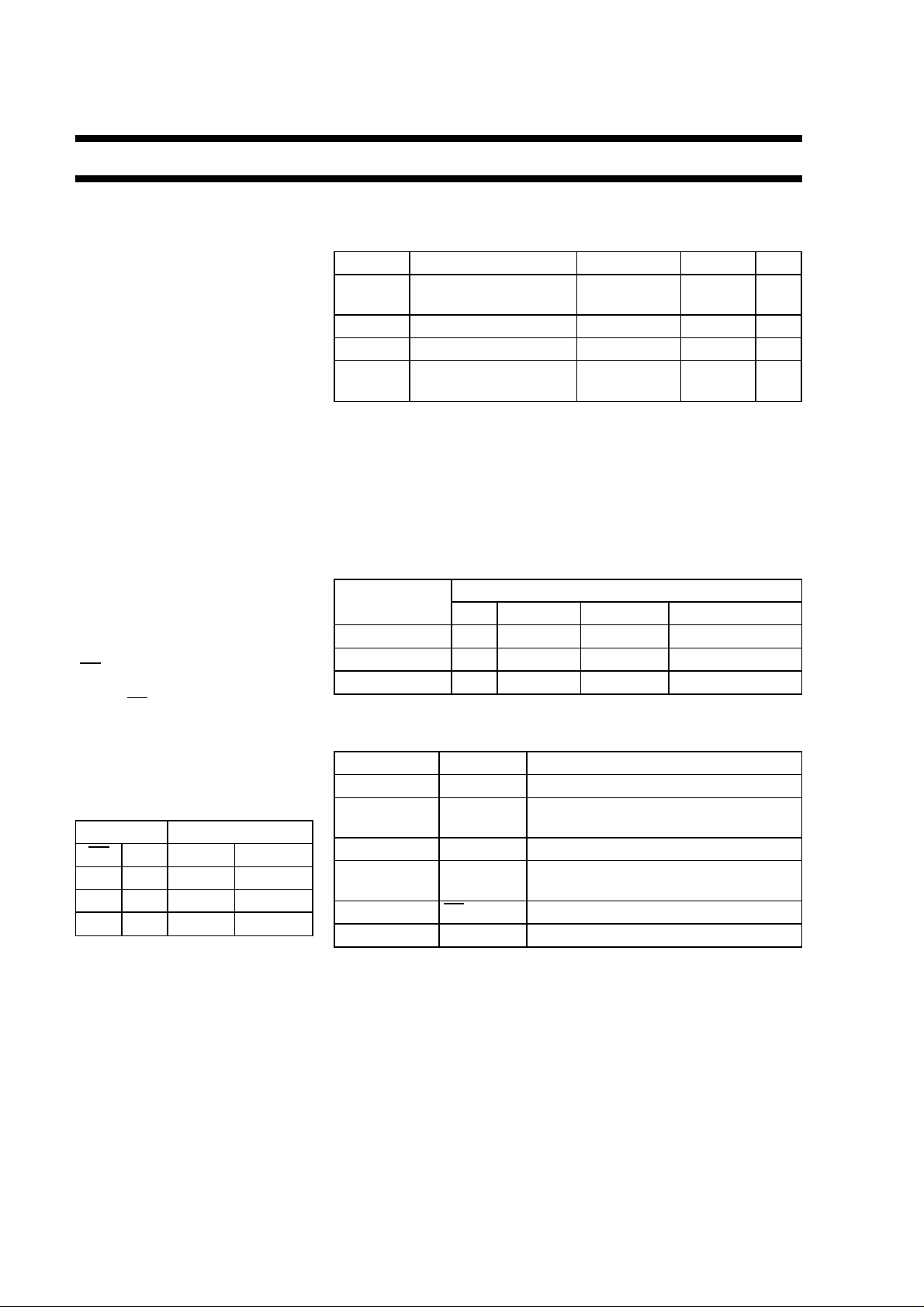
FUNCTION TABLE
INPUTS INPUTS/OUTPUT
OE DIR A
n
B
n
L L A = B inputs
L H inputs B = A
H X Z Z
H = HIGH voltage level
L = LOW voltage level
X = don’t care
Z = high impedance OFF-state
QUICK REFERENCE DATA
GND = 0 V; T
= 25 °C; tr= tf≤ 2.5 ns
amb
SYMBOL PARAMETER CONDITIONS TYPICAL UNIT
t
PHL/tPLH
C
I
C
I/O
C
PD
propagation delay
to Bn; Bnto A
A
n
n
input capacitance 5.0 pF
input/output capacitance 10 pF
power dissipation
capacitance per buffer
CL= 50 pF
= 3.3 V
V
CC
notes 1 and 2
4.1 ns
40 pF
Notes to the quick reference data
1. C
2. The condition is V
is used to determine the dynamic power dissipation (PDin µW):
PD
P
= CPDx V
D
f
= input frequency in MHz; CL= output load capacity in pF;
i
f
= output frequency in MHz; VCC= supply voltage in V;
o
Σ (C
x V
L
2
x fi+ Σ (CLx V
CC
2
x fo) = sum of outputs.
CC
= GND to VCC.
I
2
x fo) where:
CC
ORDERING INFORMATION
TYPE NUMBER
PINS PACKAGE MATERIAL CODE
PACKAGES
74LVC245D 20 SO plastic SO20/SOT163A
74LVC245DB 20 SSOP plastic SSOP20/SOT339
74LVC245PW 20 TSSOP plastic SSOP20/SOT360
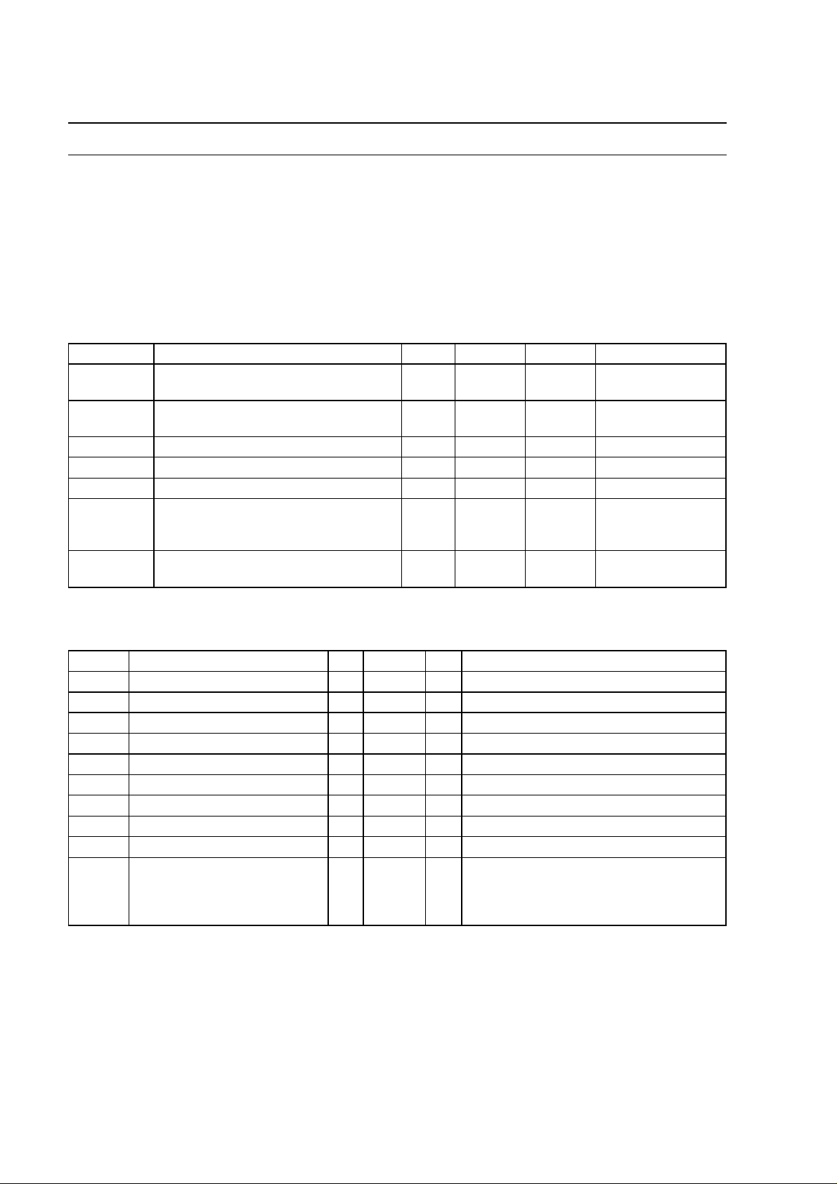
PINNING
PIN SYMBOL NAME AND FUNCTION
1 DIR direction control
2, 3, 4, 5, 6,
7, 8, 9
A0to A
data inputs/outputs
7
10 GND ground (0 V)
18, 17, 16, 15,
14, 13, 12, 11
B0to B
data inputs/outputs
7
19 OE output enable input (active LOW)
20 V
CC
positive supply voltage
April 1994 1
Philips Semiconductors Product Specification
1
2
3
4
5
6
7
8
9
10
DIR
A
0
A
1
A
2
A
3
A
4
A
5
A
6
A
7
GND B
7
B
6
B
5
B
4
B
3
B
2
B
1
B
0
OE
V
CC
20
19
18
17
16
15
14
13
12
11
245
2
1
A
0
DIR
18
19
B
0
OE
3
A
1
17
B
1
4
A
2
16
B
2
5
A
3
15
B
3
6
A
4
14
B
4
7
A
5
13
B
5
8
A
6
12
B
6
9
A
7
11
B
7
G3
3EN1
3EN2
19
1
1
2
18
2
3
17
4
16
5
15
6
14
7
13
8
12
9
11
Octal bus transceiver with direction pin; 3-state 74LVC245
Fig.1 Pin configuration.
Fig.3 IEC logic symbol.
Fig.2 Logic symbol.
April 1994 2
Philips Semiconductors Product Specification
Octal bus transceiver with direction pin; 3-state 74LVC245
FAMILY DESCRIPTION
The LVC family comprises very fast
low-power logic ICs fabricated in a
sub-micron CMOS process.
LVC ICs with 3.3 V ±0.3 V supply
operate at the same speed as FAST
bipolar logic and consumes only
a fraction of the power. The LVC
family functions with supply
voltages down to 2.7 V. The
reduction from the conventional
5.0 V to 3.3 V reduces the output
swing leading to a much lower
dynamic power dissipation. Pin and
function compatibility with FAST
ensures an easy transfer of
existing systems into new 3.3 V
systems.
RECOMMENDED OPERATING CONDITIONS FOR THE LVC FAMILY
SYMBOL PARAMETER MIN. MAX. UNIT CONDITIONS
V
V
V
V
V
T
tr, t
CC
CC
I
I/O
O
amb
f
DC supply voltage (for max. speed
performance)
DC supply voltage (for low-voltage
applications)
2.7 3.6 V
1.2 3.6 V
DC input voltage range 0 5.5 V
DC input voltage range for I/Os 0 V
DC output voltage range 0 V
operating ambient temperature range in
free air
input rise and fall times
−40 +85 °C
0
0
20
10
CC
CC
ns/V
V
V
see DC and AC
characteristics per
device
VCC= 1.2 to 2.7 V
V
= 2.7 to 3.6 V
CC
LIMITING VALUES FOR THE LVC FAMILY (Note 1)
In accordance with the Absolute Maximum Rating System (IEC 134)
Voltages are referenced to GND (ground = 0 V)
SYMBOL PARAMETER MIN. MAX. UNIT CONDITIONS
V
I
V
V
I
V
I
I
T
CC
IK
I
I/O
OK
O
O
GND
stg
DC supply voltage −0.5 +4.6 V
DC input diode current − −50 mA VI< 0
DC input voltage −0.5 +5.5 V note 2
DC input voltage range for I/Os −0.5 VCC+ 0.5 V
DC output diode current − ±50 mA VO> VCCor VO< 0
DC output voltage −0.5 VCC+ 0.5 V note 2
DC output source or sink current − ±50 mA VO= 0 to V
, I
DC VCCor GND current − ±100 mA
CC
storage temperature range −60 +150 °C
CC
power dissipation per package
P
tot
- plastic mini-pack (SO)
- plastic shrink mini-pack
−
−
500
500mWmW
above + 70°C derate linearly with 8 mW/K
above + 60°C derate linearly with 5.5 mW/K
(SSOP and TSSOP)
Notes to the limiting values
1. Stresses beyond those listed
may cause permanent damage to
the device. These are stress
ratings only and functional
operation of the device at these
those under ’recommended
operating conditions’ is not implied.
Exposure to absolute maximum
rated conditions for extended
periods may affect device reliability.
or any other conditions beyond
April 1994 3
2. The input and output voltage
ratings may be exceeded if the
input and output current ratings
are observed.
 Loading...