

Philips 74lvc241a DATASHEETS

INTEGRATED CIRCUITS
74LVC241A
Octal buffer/line driver with 5-volt tolerant
inputs/outputs (3-State)
Product specification
Supersedes data of 1997 Jul 29
IC24 Data Handbook
1998 May 20
Philips Semiconductors Product specification
Octal buffer/line driver with 5-volt tolerant
inputs/outputs (3-State)
FEA TURES
•5-Volt tolerant inputs/outputs, for interfacing with 5-volt logic.
•Supply voltage range of 1.2 to 3.6 V
•In accordance with JEDEC standard no. 8-1A
•CMOS lower power consumption
•Direct interface with TTL levels
•High impedance when V
QUICK REFERENCE DATA
GND = 0 V; T
SYMBOL
t
PHL/tPLH
C
I
C
PD
= 25°C; tr = t
amb
Propagation delay
1An to 1Yn;
2An to 2Y
Input capacitance 5.0 pF
Power dissipation capacitance per buffer VCC = 3.3 V 25 pF
= 0 V
CC
≤ 2.5 ns
f
PARAMETER CONDITIONS TYPICAL UNIT
CL = 50 pF;
VCC = 3.3 V
n
74L VC241A
DESCRIPTION
The 74LVC241A is a high-performance, low-power, low-voltage,
Si-gate CMOS device and superior to most advanced CMOS
compatible TTL families.
Inputs can be driven from either 3.3 V or 5 V devices. In 3-State
operation, outputs can handle 5 V . This feature allows the use of
these devices as translators in a mixed 3.3 V/5 V environment.
The 74LVC241A is an octal non- inverting buf fer/li ne driver with 3-State
outputs. The 3-State outputs are controlled by the output enable inputs
1OE
and 2OE. Schmitt-trigger action at all inputs makes the circuit
highly tolerant for slower input rise and fall times.
3.2 ns
ORDERING INFORMATION
PACKAGES TEMPERATURE RANGE OUTSIDE NORTH AMERICA NORTH AMERICA PKG. DWG. #
20-Pin Plastic SO –40°C to +85°C 74LVC241A D 74LVC241A D SOT163-1
20-Pin Plastic SSOP Type II –40°C to +85°C 74LVC241A DB 74LVC241A DB SOT339-1
20-Pin Plastic TSSOP Type I –40°C to +85°C 74LVC241A PW 7LVC241APW DH SOT360-1
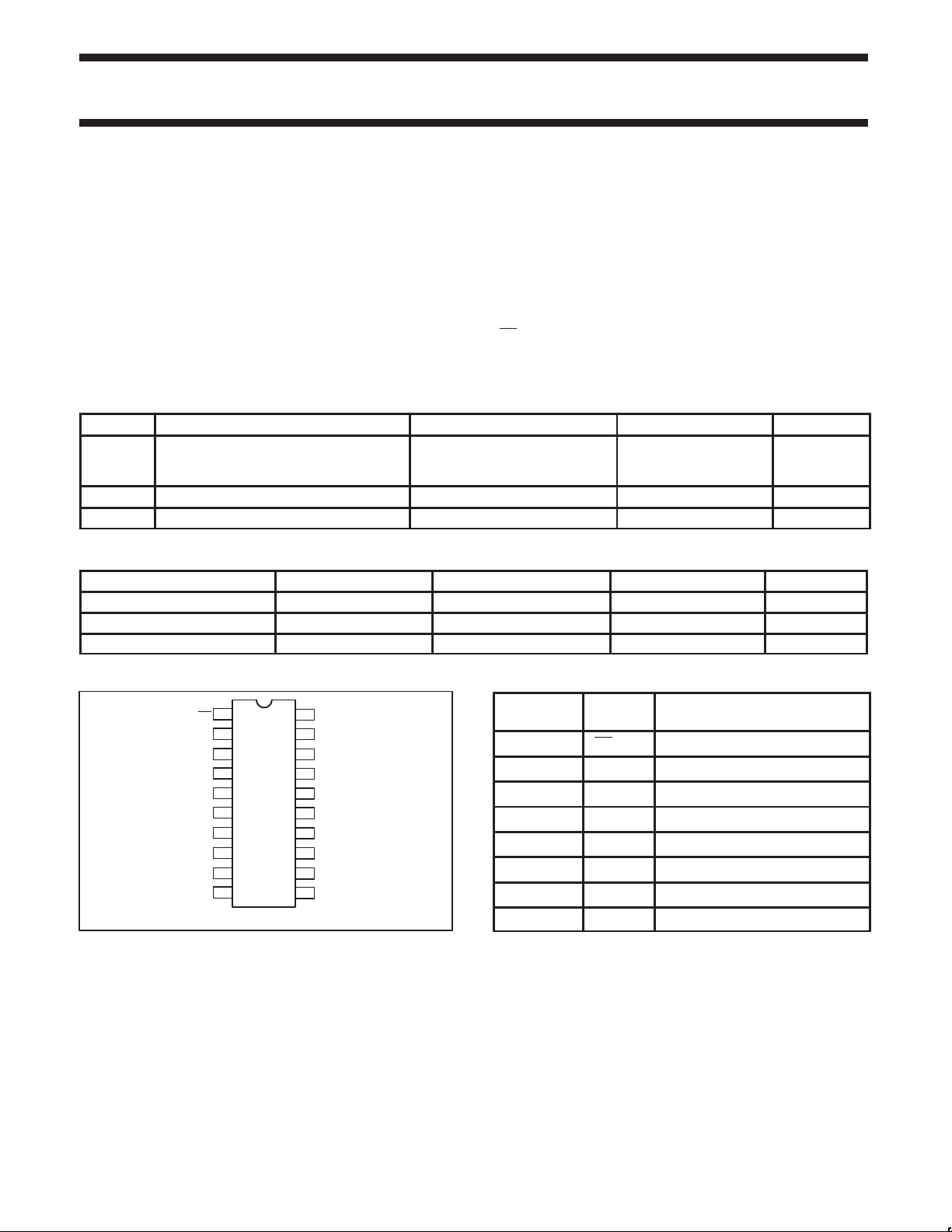
PIN CONFIGURATION
1
1OE
1A
2
0
3
2Y
0
4
1A
1
5
2Y
1
6
1A
2
7
2Y
2
8
1A
3
9
2Y
3
10
GND
20
V
19
2OE
18
1Y
17
2A
16
1Y
15
2A
14
1Y
13
2A
1Y
12
2A
11
SV00614
CC
0
0
1
1
2
2
3
3
PIN DESCRIPTION
PIN
NUMBER
1 1OE Output enable input (active LOW)
2, 4, 6, 8 1A0 to 1A3Data inputs
3, 5, 7, 9 2Y0 to 2Y3Bus outputs
10 GND Ground (0 V)
17, 15, 13, 11 2A0 to 2A3Data inputs
18, 16, 14, 12 1Y0 to 1Y3Bus outputs
19 2OE Output enable input (active HIGH)
20 V
SYMBOL FUNCTION
CC
Positive supply voltage
1998 May 20 853-2005 19419
2
Philips Semiconductors Product specification
Octal buffer/line driver with 5-volt tolerant
inputs/outputs (3-State)
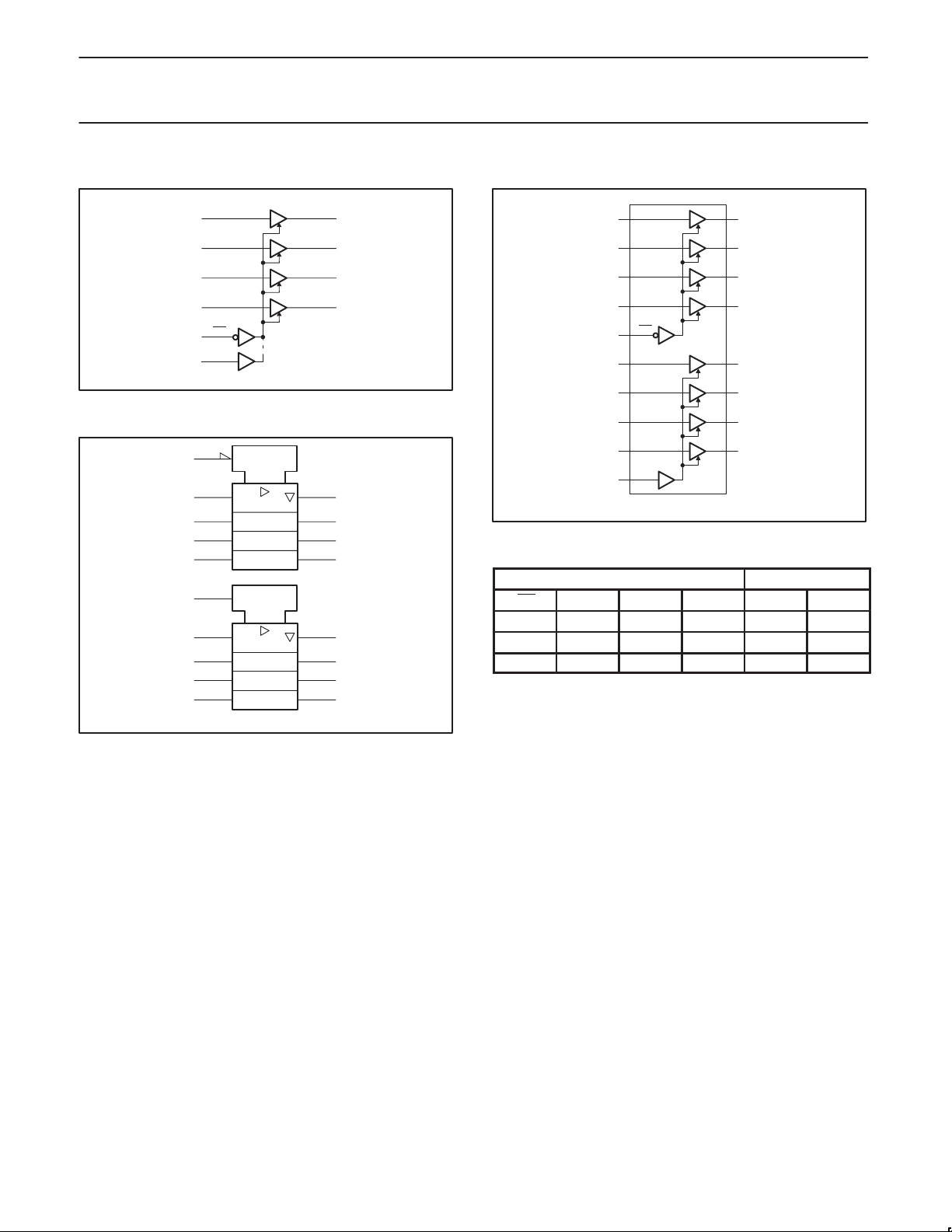
LOGIC SYMBOL
1Y
2
1A
0
2A
17
0
4
1A
1
15
2A
1
6
1A
2
13
2A
2
8
1A
3
2A
11
3
1OE1
2OE19
LOGIC SYMBOL (IEEE/IEC)
1
EN
2
4
6
8
19
EN
11
13
15
17
18
0
2Y
0
1Y
16
1
2Y
1
14
1Y
2
2Y
2
1Y
12
3
2Y
3
SV00615
SV00609
3
5
7
9
18
16
14
12
9
7
5
3
74LVC241A
FUNCTIONAL DIAGRAM
2
1A
0
4
1A
1
6
1A
2
1A
8
3
1OE1
17
2A
0
15
2A
1
13
2A
2
11
2A
3
2OE19
FUNCTION TABLE
INPUTS OUTPUT
1OE 1A
L L H L L L
L H H H H H
H X L X Z Z
NOTES:
H = HIGH voltage level
L = LOW voltage level
X = don’t care
Z = high impedance OFF-state
n
2OE 2A
1Y018
1Y
1
1Y
2
1Y
3
2Y03
2Y
1
2Y
2
2Y
3
SV00616
n
16
14
12
5
7
9
1Y
n
2Y
n
1998 May 20
3
 Loading...