

Philips 74LVC2244APW, 74LVC2244AD Datasheet

INTEGRATED CIRCUITS
DATA SH EET
74LVC2244A
Octal buffer/line driver with 30 Ω
series termination resistors; 5 V
input/output tolerant; 3-state
Product specification
File under Integrated Circuits, IC24
1999 Sep 30
Philips Semiconductors Product specification
Octal buffer/line driver with 30 Ω series termination
resistors; 5 V input/output tolerant; 3-state
FEATURES
• 5 V tolerant inputs/outputs for interfacing with 5 V logic
• Wide supply voltage range of 1.2 to 3.6 V
• CMOS low power consumption
• Direct interface with TTL levels
• Integrated 30 Ω termination resistors.
QUICK REFERENCE DATA
Ground = 0 V; T
=25°C; tr=tf≤2.5 ns.
amb
DESCRIPTION
The 74LVC2244A is a high-performance, low-power,
low-voltage, Si-gate CMOS device, superior to most
advanced CMOS compatible TTL families.
Inputs can be driven from either 3.3 or 5 V devices. In
3-state operation,outputs can handle 5 V. These features
allow the use of these devices as translators in a mixed
3.3/5 V environment.
The 74LVC2244A is an octal non-inverting buffer/line
driver with 3-state outputs. The 3-state outputs are
controlled by the output enable inputs 1OE and 2OE. A
HIGH on nOE causes the outputs to assume a
high-impedance OFF-state. Schmitt-trigger action at all
inputsmakes the circuit highly tolerant for slower input rise
and fall times. The 74LVC2244A is designed with 30 Ω
series termination resistors in both HIGH and LOW output
stages to reduce line noise.
74LVC2244A
SYMBOL PARAMETER CONDITIONS TYPICAL UNIT
t
PHL/tPLH
C
I
C
PD
propagation delay 1Anto 1Yn; 2Anto 2Y
n
CL= 50 pF; VCC= 3.3 V 4.0 ns
input capacitance 5.0 pF
power dissipation capacitance per buffer VI= GND to VCC; note 1 25 pF
Note
1. C
is used to determine the dynamic power dissipation (PDin µW).
PD
PD=CPD× V
2
× fi+ Σ(CL× V
CC
2
× fo) where:
CC
fi= input frequency in MHz;
fo= output frequency in MHz;
CL= output load capacitance in pF;
= supply voltage in Volts;
V
CC
Σ(CL× V
2
× fo) = sum of the outputs.
CC
1999 Sep 30 2
Philips Semiconductors Product specification
Octal buffer/line driver with 30 Ω series termination
74LVC2244A
resistors; 5 V input/output tolerant; 3-state
FUNCTION TABLE
See note 1.
INPUT OUTPUT
OE nA
n
n
LL L
LH H
HX Z
Note
1. H = HIGH voltage level;
L = LOW voltage level;
X = don’t care;
Z = high-impedance OFF-state.
ORDERING INFORMATION
PACKAGE
OUTSIDE NORTH
AMERICA
NORTH AMERICA
TEMPERATURE
RANGE
PINS PACKAGE MATERIAL CODE
74LVC2244AD 74LVC2244AD −40 to +85 °C 20 SO plastic SOT163-1
74LVC2244ADB 74LVC2244ADB 20 SSOP plastic SOT339-1
74LVC2244APW 74LVC2244APW DH 20 TSSOP plastic SOT360-1
nY
n
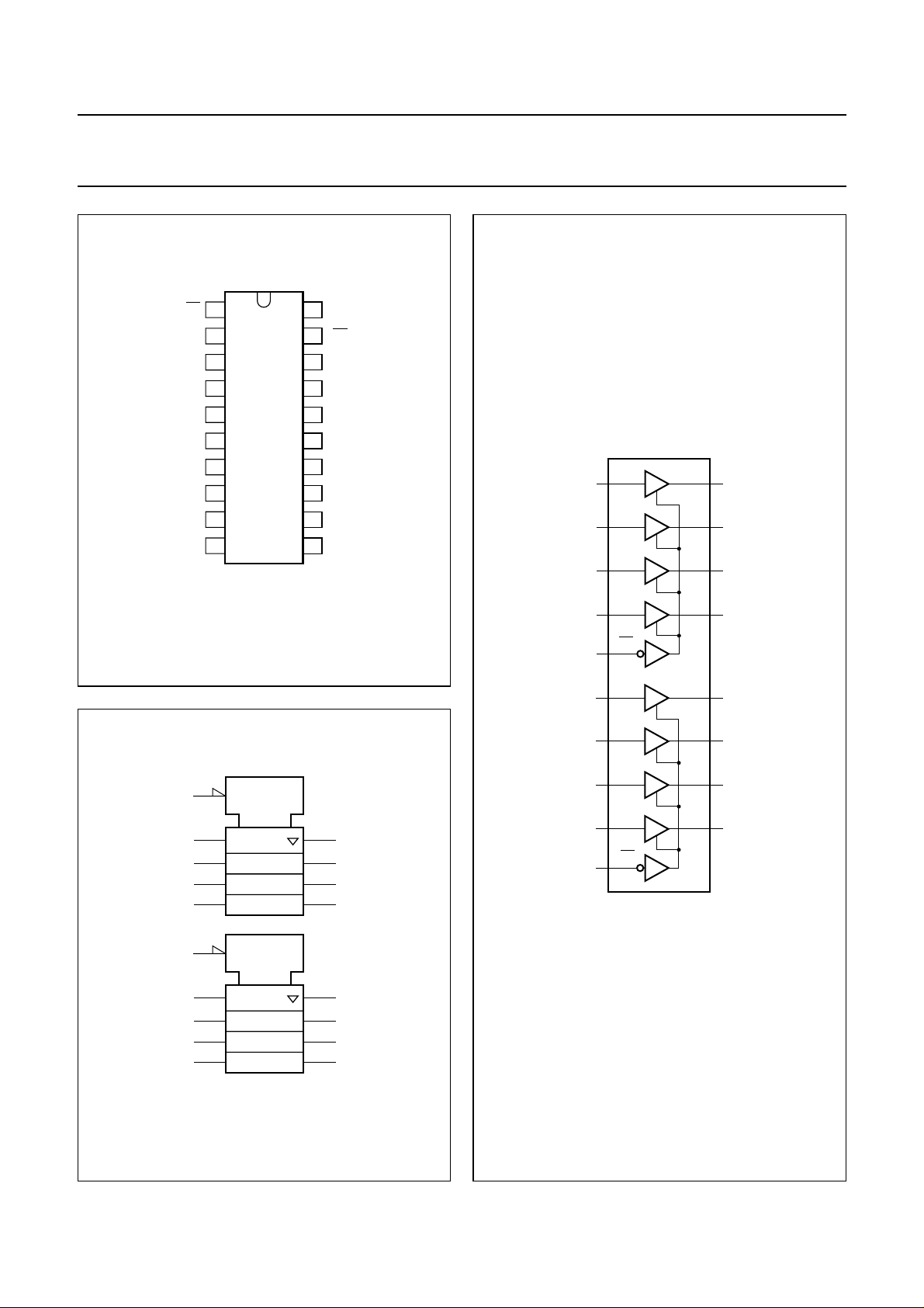
PINNING
PIN SYMBOL DESCRIPTION
11
2, 4, 6, 8 1A
3, 5, 7, 9 2Y
OE output enable input (active LOW)
to 1A
0
to 2Y
0
3
3
data inputs
bus outputs
10 GND ground (0 V)
11, 13, 15, 17 2A
12, 14, 16, 18 1Y
19 2
20 V
to 2A
3
to 1Y
3
0
0
data inputs
bus outputs
OE output enable input (active LOW)
CC
DC supply voltage
1999 Sep 30 3
Philips Semiconductors Product specification
Octal buffer/line driver with 30 Ω series termination
resistors; 5 V input/output tolerant; 3-state
handbook, halfpage
1OE
1A
2Y
1A
2Y
1A
2Y
1A
2Y
GND
1
2
0
3
0
4
1
5
1
2
2
3
3
2244
6
7
8
9
10
MNA357
V
20
CC
19
2OE
1Y
18
0
2A
17
0
1Y
16
1
2A
15
1
1Y
14
2
2A
13
2
1Y
12
3
2A
11
3
handbook, halfpage
74LVC2244A
1A
0
2
1A
1
4
1A
2
6
1Y
1Y
1Y
0
18
1
16
2
14
handbook, halfpage
Fig.1 Pin configuration.
1
EN
2
4
6
8
19
EN
17
15
13
11
MNA359
18
16
14
12
3
5
7
9
1A
3
8
1OE
1
2A
2A
2A
2A
2OE
0
1
2
3
17
15
13
11
19
1Y
2Y
2Y
2Y
2Y
MNA360
3
12
0
3
1
5
2
7
3
9
1999 Sep 30 4
Fig.2 Functional diagram.Fig.3 IEC logic symbol.
Philips Semiconductors Product specification
Octal buffer/line driver with 30 Ω series termination
74LVC2244A
resistors; 5 V input/output tolerant; 3-state
RECOMMENDED OPERATING CONDITIONS
SYMBOL PARAMETER CONDITIONS MIN. MAX. UNIT
V
CC
V
I
V
O
T
amb
t
r,tf
LIMITING VALUES
In accordance with the Absolute Maximum Rating System (IEC 134). Voltages are referenced to GND (ground = 0 V).
DC supply voltage
for max. speed performance 2.7 3.6 V
for low-voltage applications 1.2 3.6 V
DC input voltage 0 5.5 V
DC output voltage
output HIGH or LOW state 0 V
CC
V
3-state 0 5.5 V
operating ambient temperature see DC and AC characteristics per
−40 +85 °C
device
input rise and fall times VCC= 1.2 to 2.7 V 0 20 ns/V
V
= 2.7 to 3.6 V 0 10
CC
SYMBOL PARAMETER CONDITIONS MIN. MAX. UNIT
V
CC
I
IK
V
I
I
OK
V
O
DC supply voltage −0.5 +6.5 V
DC input diode current VI<0 −−50 mA
DC input voltage note 1 −0.5 +5.5 V
DC output diode current VO>VCC or VO<0 −±50 mA
DC output voltage
output HIGH or LOW note 1 −0.5 V
+ 0.5 V
CC
output 3-state note 1 −0.5 +6.5 V
I
O
I
, I
CC
T
stg
P
tot
DC output diode current VO=0toV
DC VCC or GND current −±100 mA
GND
CC
−±50 mA
storage temperature −65 +150 °C
power dissipation per package
plastic mini-pack (SO) note 2 − 500 mW
plastic shrink mini-pack (SSOP and
note 3 − 500 mW
TSSOP)
Notes
1. The input and output voltage ratings may be exceeded if the input and output current ratings are observed.
2. For SO package: above 70 °C the value of P
3. For SSOP and TSSOP package: above 60 °C the value of P
derates linearly with 8 mW/K.
tot
derates linearly with 5.5 mW/K.
tot
1999 Sep 30 5
 Loading...