

Page 1

INTEGRATED CIRCUITS
DATA SH EET
74LVC163
Presettable synchronous 4-bit
binary counter; synchronous reset
Product specification
Supersedes data of 2003 June 02
2004 May 05
Page 2

Philips Semiconductors Product specification
Presettable synchronous 4-bit binary
counter; synchronous reset
FEATURES
• Wide supply voltage range from 1.2 V to 3.6 V
• Complies with JEDEC standard JESD8-B/JESD36
• Inputs accept voltages up to 5.5 V
• CMOS low power consumption
• Direct interface with TTL levels
• Synchronous reset
• Synchronous counting and loading
• Two count enable inputs for n-bit cascading
• Positive edge-triggered clock.
• ESD protection:
– HBM EIA/JESD22-A114-B exceeds 2000 V
– MM EIA/JESD22-A115-A exceeds 200 V.
• Specified from−40 °C to +85 °C and −40 °C to +125 °C.
DESCRIPTION
The 74LVC163 is a high-performance, low-power,
low-voltage, Si-gate CMOS device and superior to most
advanced CMOS compatible TTL families.
The 74LVC163 is a synchronous presettable binary
counterwhichfeaturesaninternal look-head carry andcan
be used for high-speed counting. Synchronous operation
is provided by having all flip-flops clocked simultaneously
on the positive-going edge of the clock (pin CP). The
outputs (pins Q0 to Q3) of the counters may be preset to a
74LVC163
HIGH-level or LOW-level. A LOW-level at the parallel
enable input (pin PE) disables the counting action and
causes the data at the data inputs (pins D0 to D3) to be
loaded into the counter on the positive-going edge of the
clock (provided that the set-up and hold time requirements
forPEaremet).Presettakesplace regardless of the levels
at count enable inputs (pins CEP and CET). A LOW-level
at the master reset input (pin MR) sets all four outputs of
the flip-flops (pins Q0 to Q3) to LOW-level after the next
positive-going transition on the clock input (pin CP)
(provided that the set-up and hold time requirements for
PE are met). This action occurs regardless of the levels at
input pins PE, CET and CEP. This synchronous reset
featureenablesthedesignerto modify the maximumcount
with only one external NAND gate.
The look-ahead carry simplifies serial cascading of the
counters. Both count enable inputs (pins CEP and CET)
must be HIGH to count. The CET input is fed forward to
enable the terminal count output (pin TC). The TC output
thus enabled will produce a HIGH output pulse of a
durationapproximatelyequaltoa HIGH-level output ofQ0.
Thispulsecanbeusedtoenablethenextcascadedstage.
The maximum clock frequency for the cascaded counters
is determined by t
(set-up time CEP to CP) according to the
formula: .f
max
(propagation delay CP to TC) and t
PHL
=
1
------------------------------------ t
PHL max()tsu
+
su
2004 May 05 2
Page 3
Philips Semiconductors Product specification
Presettable synchronous 4-bit binary
74LVC163
counter; synchronous reset
QUICK REFERENCE DATA
GND = 0 V; T
SYMBOL PARAMETER CONDITIONS TYPICAL UNIT
t
PHL/tPLH
f
clk(max)
C
I
C
PD
Notes
1. C
is used to determine the dynamic power dissipation (PD in µW).
PD
PD=CPD× V
fi= input frequency in MHz;
fo= output frequency in MHz;
CL= output load capacitance in pF;
VCC= supply voltage in Volts;
N = total load switching outputs;
Σ(CL× V
2. The condition is VI= GND to VCC.
=25°C; tr=tf≤ 2.5 ns.
amb
propagation delay: CL= 50 pF; VCC= 3.3 V
CP to Qn 4.0 ns
CP to TC 4.6 ns
CET to TC 3.5 ns
maximum clock frequency 200 MHz
input capacitance 5.0 pF
power dissipation capacitance per gate notes 1 and 2 17 pF
2
× fi× N+Σ(CL× V
CC
2
× fo) = sum of the outputs.
CC
2
× fo) where:
CC
ORDERING INFORMATION
TYPE NUMBER
TEMPERATURE
RANGE
PINS PACKAGE MATERIAL CODE
74LVC163D −40 °C to +125 °C 16 SO16 plastic SOT109-1
74LVC163DB −40 °C to +125 °C 16 SSOP16 plastic SOT338-1
74LVC163PW −40 °C to +125 °C 16 TSSOP16 plastic SOT403-1
74LVC163BQ −40 °C to +125 °C 16 DHVQFN16 plastic SOT763-1
2004 May 05 3
Page 4
Philips Semiconductors Product specification
Presettable synchronous 4-bit binary
74LVC163
counter; synchronous reset
FUNCTION TABLE
See note 1.
OPERATING
MODES
Reset (clear) l ↑ XXXXLL
Parallel load h ↑ XX l l LL
Count h ↑ h h h X count *
Hold
(do nothing)
Note
1. * = the TC output is HIGH when CET is HIGH and the counter is at terminal count (HHHH).
H = HIGH voltage level.
h = HIGH voltage level one set-up time prior to the LOW-to-HIGH clock transition.
L = LOW voltage level.
l = LOW voltage level one set-up time prior to the LOW-to-HIGH clock transition.
q = lower case letters indicate the state of the referenced output one set-up time prior to the LOW-to-HIGH clock
transition.
X = don’t care.
↑=LOW-to-HIGH clock transition.
MR CP CEP CET PE Dn Qn TC
h ↑ XX l hH*
hXlXhXqn*
hXXl hXqnL
INPUT OUTPUT
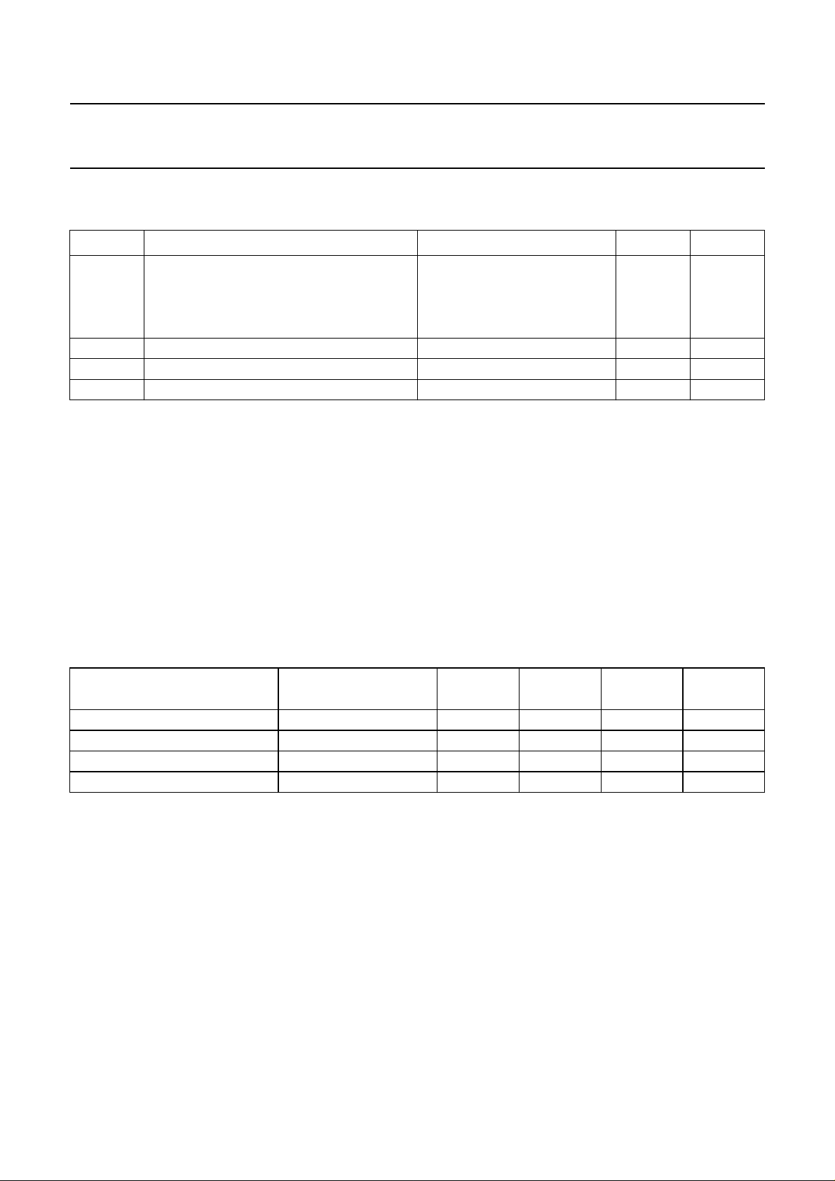
PINNING
PIN SYMBOL DESCRIPTION
1 MR synchronous master reset (active LOW)
2 CP clock input (LOW-to-HIGH, edge-triggered)
3 D0 data input
4 D1 data input
5 D2 data input
6 D3 data input
7 CEP count enable input
8 GND ground (0 V)
9 PE parallel enable input (active LOW)
10 CET count enable carry input
11 Q3 flip-flop output
12 Q2 flip-flop output
13 Q1 flip-flop output
14 Q0 flip-flop output
15 TC terminal count output
16 V
CC
supply voltage
2004 May 05 4
Page 5
Philips Semiconductors Product specification
Presettable synchronous 4-bit binary
counter; synchronous reset
MR V
1
CP TC
2
D0 Q0
3
D1 Q1
4
163
D2 Q2
5
D3 Q3
6
CEP CET
7
GND PE
8
001aaa770
16
CC
15
14
13
12
11
10
9
terminal 1
index area
CP TC
D0 Q0
D1 Q1
D2 Q2
D3 Q3
CEP CET
MR
1
2 15
3 14
4 13
163
5 12
6 11
7 10
Transparent top view
GND
(1)
8
GND
V
16
9
PE
CC
001aaa740
74LVC163
Fig.1 Pin configuration SO16 and (T)SSOP16.
handbook, halfpage
3
4
5
6
9
D0
D1
D2
D3
PE
CEP7CET
15
TC
Q0
Q1
Q2
Q3
MR
CP
MNA905
10
1
2
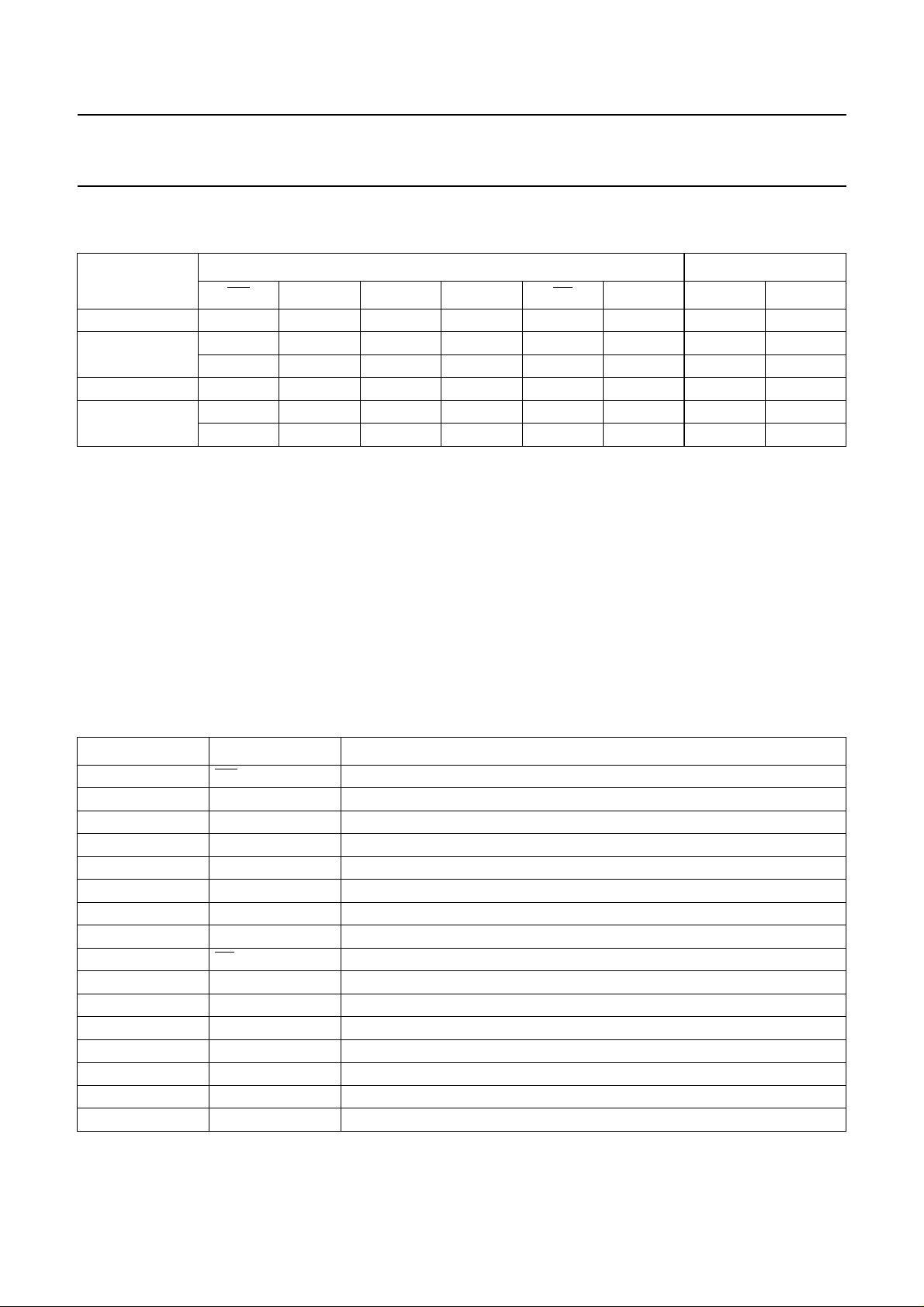
(1) The die substrate is attached to the exposed die pad using
conductivedie attach material.It cannot beused asasupply pin
or input.
Fig.2 Pin configuration DHVQFN16
handbook, halfpage
14
13
12
11
1
9
7
10
2
3
4
5
6
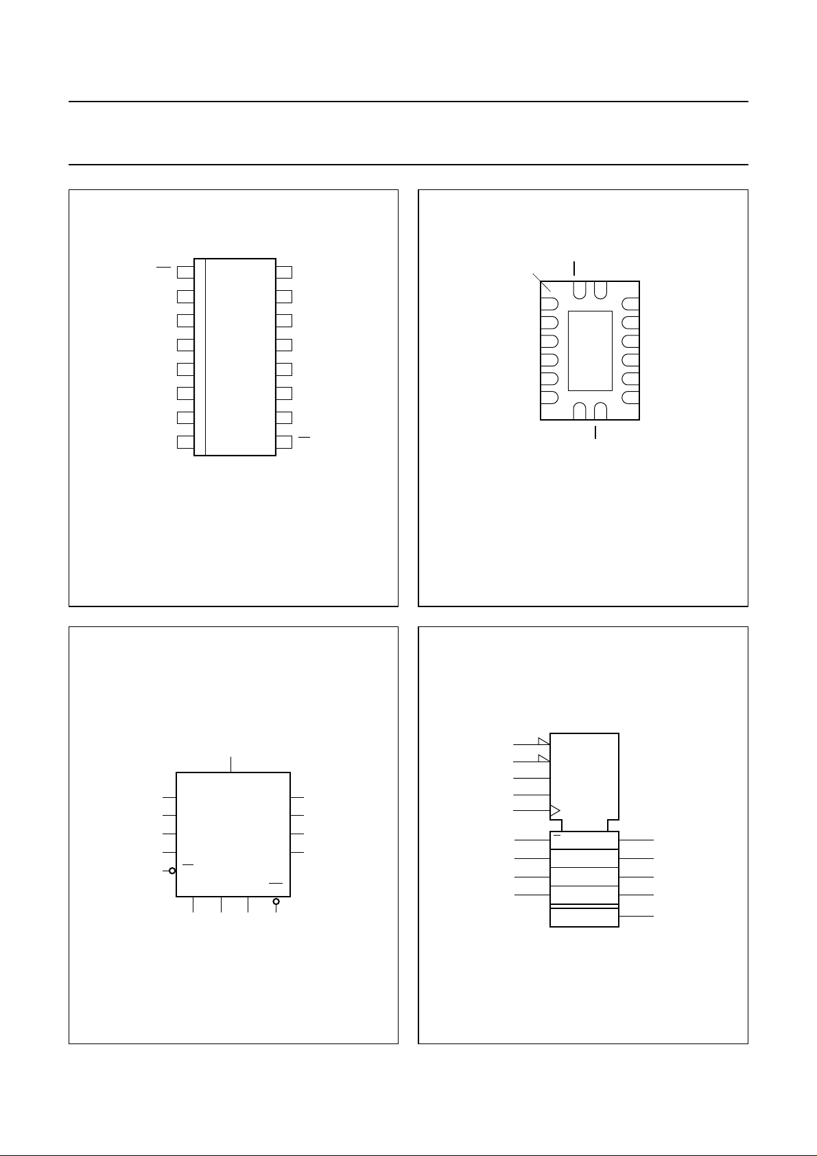
CTR4
R
M1
G3
G4
C2 /1,3,4+
1,2D
4 CT = 15
14
13
12
11
15
MNA906
Fig.3 Logic symbol.
2004 May 05 5
Fig.4 Logic symbol (IEEE/IEC).
Page 6
Philips Semiconductors Product specification
Presettable synchronous 4-bit binary
counter; synchronous reset
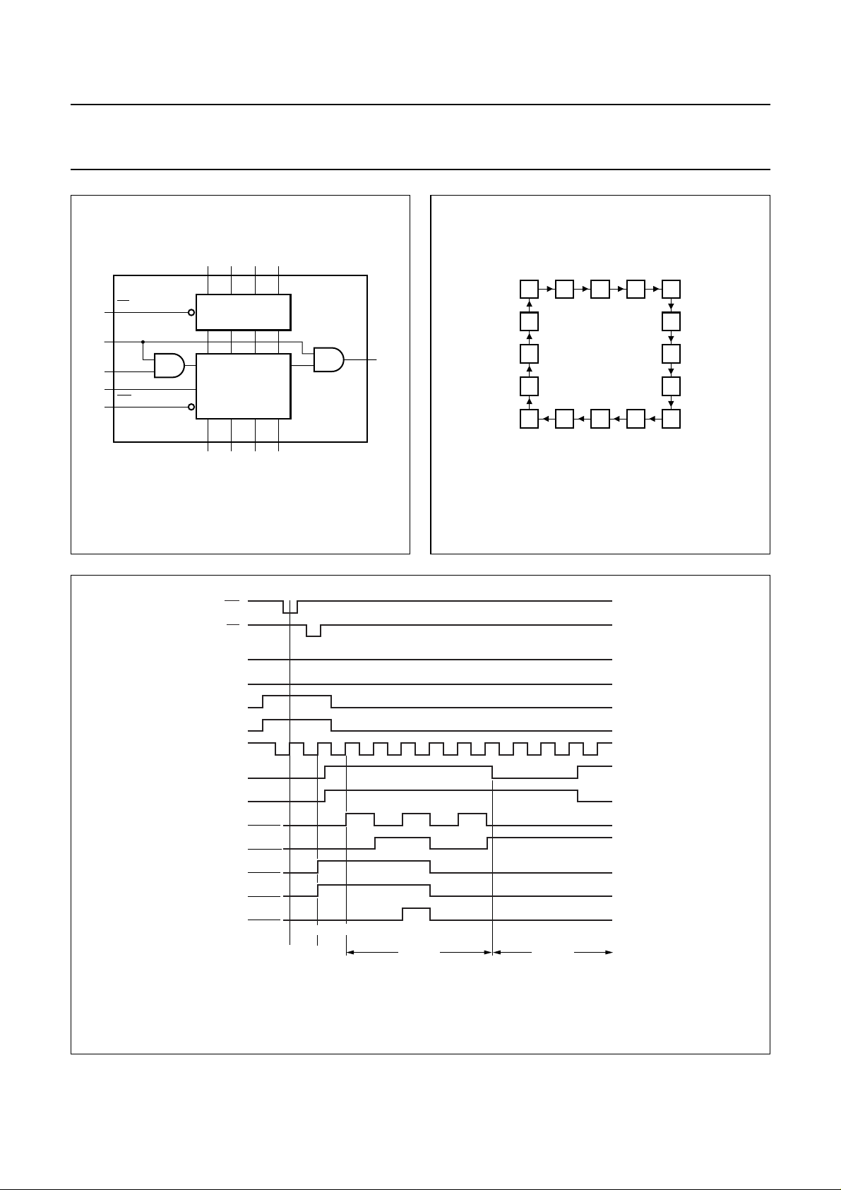
handbook, halfpage
PE
9
CET
10
CEP
7
CP
2
MR
1
3456
D0 D1 D2 D3
PARALLEL LOAD
CIRCUITRY
BINARY
COUNTER
Q0 Q1 Q2 Q3
14 13 12 11
Fig.5 Functional diagram.
TC
MNA907
74LVC163
handbook, halfpage
15
0
1 2 3 4
15
14
13
11 10 9 8
12
Fig.6 State diagram.
5
6
7
MNA908
handbook, full pagewidth
Typical timing sequence: Reset outputs to zero; preset to binary twelve; count to thirteen, fourteen, fifteen, zero, one and two; inhibit.
MR
PE
D0
D1
D2
D3
CP
CEP
CET
Q0
Q1
Q2
Q3
TC
12 13 14 15 0 1 2
RESET PRESET
INHIBITCOUNT
MGU760
Fig.7 Timing sequence.
2004 May 05 6
Page 7
This text is here in white to force landscape pages to be rotated correctly when browsing through the pdf in the Acrobat reader.This text is here in
_white to force landscape pages to be rotated correctly when browsing through the pdf in the Acrobat reader.This text is here inThis text is here in
white to force landscape pages to be rotated correctly when browsing through the pdf in the Acrobat reader. white to force landscape pages to be ...
2004 May 05 7
2004 May 05 7
D0 D1 D2 D3
CET
CEP
handbook, full pagewidth
Philips Semiconductors Product specification
Philips Semiconductors Product specification
Presettable synchronous 4-bit binary
counter; synchronous reset
Presettable synchronous 4-bit binary
counter; synchronous reset
PE
MR
CP
D
CP
FF0
Q
Q
Q0
D
CP
FF1
Q
Q
Q1 Q2 Q3 TC
D
CP
FF2
Q
Q
D
CP
FF3
Q
Q
74LVC163
74LVC163
MGU761
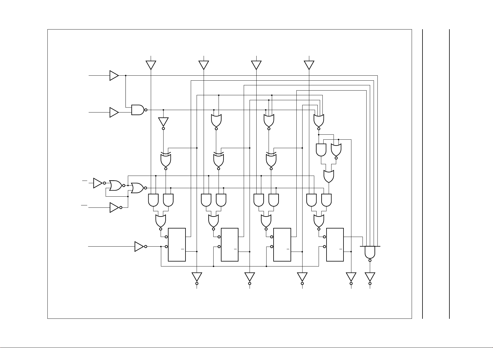
Fig.8 Logic diagram.
Page 8

Philips Semiconductors Product specification
Presettable synchronous 4-bit binary
74LVC163
counter; synchronous reset
RECOMMENDED OPERATING CONDITIONS
SYMBOL PARAMETER CONDITIONS MIN. MAX. UNIT
V
CC
V
I
V
O
T
amb
tr, t
f
LIMITING VALUES
In accordance with the Absolute Maximum Rating System (IEC 60134); voltages are referenced to GND (ground = 0 V).
SYMBOL PARAMETER CONDITIONS MIN. MAX. UNIT
V
CC
I
IK
V
I
I
OK
V
O
I
O
ICC, I
GND
T
stg
P
tot
supply voltage for maximum speed performance 2.7 3.6 V
for low-voltage applications 1.2 3.6 V
input voltage 0 5.5 V
output voltage 0 V
CC
V
operating ambient temperature in free air −40 +125 °C
input rise and fall times VCC= 1.2 V to 2.7 V 0 20 ns/V
VCC= 2.7 V to 3.6 V 0 10 ns/V
supply voltage −0.5 +6.5 V
input diode current VI<0V −−50 mA
input voltage note 1 −0.5 +6.5 V
output diode current VO>VCC or VO<0V −±50 mA
output voltage note 1 −0.5 VCC+ 0.5 V
output source or sink current VO=0VtoV
CC
−±50 mA
VCC or GND current −±100 mA
storage temperature −65 +150 °C
power dissipation T
= −40 °C to +125 °C; note 2 − 500 mW
amb
Notes
1. The input and output voltage ratings may be exceeded if the input and output current ratings are observed.
2. For SO16 packages: above 70 °C the value of P
For SSOP16 and TSSOP16 packages: above 60 °C the value of P
For DHVQFN16 packages: above 60 °C the value of P
derates linearly with 8 mW/K.
tot
derates linearly with 5.5 mW/K.
tot
derates linearly with 4.5 mW/K.
tot
2004 May 05 8
Page 9

Philips Semiconductors Product specification
Presettable synchronous 4-bit binary
counter; synchronous reset
DC CHARACTERISTICS
At recommended operating conditions; voltages are referenced to GND (ground = 0 V).
SYMBOL PARAMETER
T
= −40 °C to +85 °C
amb
V
IH
HIGH-level input
voltage
V
IL
LOW-level input
voltage
V
OH
HIGH-level output
voltage
V
OL
LOW-level output
voltage
I
LI
input leakage
current
I
CC
quiescent supply
current
∆I
CC
additional quiescent
supply current per
input pin
TEST CONDITIONS
MIN. TYP.
OTHER VCC (V)
1.2 V
CC
2.7 to 3.6 2.0 −−V
1.2 −−GND V
2.7 to 3.6 −−0.8 V
VI=VIHor V
IL
IO= −100 µA 2.7 to 3.6 VCC− 0.2 V
IO= −12 mA 2.7 VCC− 0.5 −−V
IO= −18 mA 3.0 VCC− 0.6 −−V
IO= −24 mA 3.0 VCC− 0.8 −−V
VI=VIHor V
IL
IO= 100 µA 2.7 to 3.6 − GND 0.2 V
IO=12mA 2.7 −−0.4 V
IO=24mA 3.0 −−0.55 V
VI= 5.5 Vor GND 3.6 −±0.1 ±5 µA
VI=VCCor GND;
3.6 − 0.1 10 µA
IO=0A
VI=VCC− 0.6 V;
2.7 to 3.6 − 5 500 µA
IO=0A
74LVC163
(1)
−−V
CC
MAX. UNIT
− V
2004 May 05 9
Page 10

Philips Semiconductors Product specification
Presettable synchronous 4-bit binary
counter; synchronous reset
SYMBOL PARAMETER
T
= −40 °C to +125 °C
amb
V
IH
HIGH-level input
voltage
V
IL
LOW-level input
voltage
V
OH
HIGH-level output
voltage
V
OL
LOW-level output
voltage
I
LI
input leakage
current
I
CC
quiescent supply
current
∆I
CC
additional quiescent
supply current per
input pin
TEST CONDITIONS
OTHER VCC (V)
VI=VIHor V
IL
IO= −100 µA 2.7 to 3.6 VCC− 0.3 −−V
IO= −12 mA 2.7 VCC− 0.65 −−V
IO= −18 mA 3.0 VCC− 0.75 −−V
IO= −24 mA 3.0 VCC− 1 −−V
VI=VIHor V
IL
IO= 100 µA 2.7 to 3.6 −−0.3 V
IO=12mA 2.7 −−0.6 V
IO=24mA 3.0 −−0.8 V
VI= 5.5 Vor GND 3.6 −−±20 µA
VI=VCCor GND;
IO=0A
VI=VCC− 0.6 V;
IO=0A
74LVC163
MIN. TYP.
1.2 V
CC
2.7 to 3.6 2.0 −−V
1.2 −−GND V
2.7 to 3.6 −−0.8 V
3.6 −−40 µA
2.7 to 3.6 −−5000 µA
(1)
MAX. UNIT
−−V
Note
1. Typical values are measured at VCC= 3.3 V and T
amb
=25°C.
2004 May 05 10
Page 11

Philips Semiconductors Product specification
Presettable synchronous 4-bit binary
counter; synchronous reset
AC CHARACTERISTICS
GND = 0 V; tr=tf≤ 2.5 ns; CL= 50 pF; RL= 500 Ω.
SYMBOL PARAMETER
T
= −40 °C to +85 °C; note 1
amb
t
PHL/tPLH
propagation delay CP to Qn see Figs 9 and 14 1.2 − 18 − ns
propagation delay CP to TC see Figs 9 and 14 1.2 − 23 − ns
propagation delay CET to TC see Figs 10 and 14 1.2 − 16 − ns
t
W
clock pulse width
HIGH or LOW
t
su
set-up time Dn to CP see Fig.12 2.7 3.0 −−ns
set-up time MR, PE to CP see Fig.12 2.7 3.5 −−ns
set-up time CEP, CET to CP see Fig.13 2.7 5.5 −−ns
t
h
hold time Dn, PE, CEP, CET
to CP
f
max
maximum clock pulse
frequency
t
sk(0)
skew note 3 3.0 to 3.6 −−1.0 ns
WAVEFORMS V
see Fig.9 2.7 5.0 −−ns
see Figs 12 and 13 2.7 0.0 −−ns
see Fig.9 2.7 150 −−MHz
CONDITIONS
74LVC163
(V)
CC
2.7 1.5 − 7.3 ns
3.0 to 3.6 1.5 4.0
2.7 1.5 − 8.1 ns
3.0 to 3.6 1.5 4.6
2.7 1.5 − 6.9 ns
3.0 to 3.6 1.5 3.5
3.0 to 3.6 4.0 1.2
3.0 to 3.6 2.5 1.0
3.0 to 3.6 3.0 1.2
3.0 to 3.6 5.0 2.1
3.0 to 3.6 0.5 0.0
3.0 to 3.6 150 200
MIN. TYP. MAX. UNIT
(2)
7.3 ns
(2)
7.9 ns
(2)
6.4 ns
(2)
− ns
(2)
− ns
(2)
− ns
(2)
− ns
(2)
− ns
(2)
− MHz
2004 May 05 11
Page 12

Philips Semiconductors Product specification
Presettable synchronous 4-bit binary
74LVC163
counter; synchronous reset
SYMBOL PARAMETER
T
= −40 °C to +125 °C
amb
t
PHL/tPLH
propagation delay CP to Qn see Figs 9 and 14 1.2 −−−ns
propagation delay CP to TC see Figs 9 and 14 1.2 −−−ns
propagation delay CET to TC see Figs 10 and 14 1.2 −−−ns
t
W
clock pulse width
see Fig.9 2.7 5.0 −−ns
HIGH or LOW
t
su
set-up time Dn to CP see Fig.12 2.7 3.0 −−ns
set-up time MR, PE to CP see Fig.12 2.7 3.5 −−ns
set-up time CEP, CET to CP see Fig.13 2.7 5.5 −−ns
t
h
hold time Dn, PE, CEP, CET
see Figs 12 and 13 2.7 0.0 −−ns
to CP
f
max
maximum clock pulse
see Fig.9 2.7 150 −−MHz
frequency
t
sk(0)
skew note 3 3.0 to 3.6 −−1.5 ns
Notes
1. All typical values are measured at T
amb
=25°C.
2. Typical values are measured at VCC= 3.3 V.
3. Skew between any two outputs of the same package switching in the same direction. This parameter is guaranteed
by design.
CONDITIONS
WAVEFORMS V
2.7 1.5 − 9.5 ns
3.0 to 3.6 1.5 − 9.5 ns
2.7 1.5 − 10.5 ns
3.0 to 3.6 1.5 − 10.0 ns
2.7 1.5 − 9.0 ns
3.0 to 3.6 1.5 − 8.0 ns
3.0 to 3.6 4.0 −−ns
3.0 to 3.6 2.5 −−ns
3.0 to 3.6 3.0 −−ns
3.0 to 3.6 5.0 −−ns
3.0 to 3.6 0.5 −−ns
3.0 to 3.6 150 −−MHz
CC
(V)
MIN. TYP. MAX. UNIT
2004 May 05 12
Page 13

Philips Semiconductors Product specification
Presettable synchronous 4-bit binary
counter; synchronous reset
AC WAVEFORMS
handbook, full pagewidth
V
I
CP input
GND
V
OH
Qn, TC output
V
OL
VM= 1.5 V at VCC≥ 2.7 V.
VM= 0.5VCC at VCC< 2.7 V.
VOL and VOH are typical output voltage drop that occur with the output load.
V
M
t
PHL
74LVC163
1/f
max
V
M
t
W
t
PLH
V
M
MGU762
Fig.9 Clock (CP) to outputs (Qn, TC) propagation delays, the clock pulse width and the maximum clock
frequency.
GND
V
OH
V
OL
V
I
V
M
t
PHL
V
M
MGU763
t
PLH
V
M
V
M
handbook, halfpage
CET input
TC output
V
= 1.5 V at VCC≥ 2.7 V.
M
VM= 0.5VCC at VCC< 2.7 V.
VOL and VOH are typical output voltage drop that occur with the output load.
Fig.10 Input (CET) to output (TC) propagation delays.
2004 May 05 13
Page 14

Philips Semiconductors Product specification
Presettable synchronous 4-bit binary
counter; synchronous reset
GND
GND
V
I
V
M
t
V
I
su
handbook, full pagewidth
MR input
CP input
74LVC163
V
M
t
h
V
M
t
t
h
su
MGU764
The shaded areas indicate when the input is permitted to change for predictable output performance.
Fig.11 Master reset (MR) pulse width, the master reset to output (Qn, TC) propagation delays and the master
reset to clock (CP) removal times.
GND
GND
GND
V
I
V
M
t
su
t
h
V
I
V
M
t
su
t
h
V
I
V
M
V
M
t
su
t
h
V
M
t
su
t
h
V
M
MGU765
handbook, full pagewidth
PE input
CP input
Dn input
The shaded areas indicate when the input is permitted to change for predictable output performance.
Fig.12 Set-up and hold times for the input (Dn) and parallel enable input (PE).
2004 May 05 14
Page 15

Philips Semiconductors Product specification
Presettable synchronous 4-bit binary
counter; synchronous reset
GND
GND
V
I
V
M
t
t
su
V
I
h
V
M
handbook, full pagewidth
CEP, CET input
CP input
The shaded areas indicate when the input is permitted to change for predictable output performance.
74LVC163
V
M
t
t
su
h
V
M
MGU766
Fig.13 CEP and CET set-up and hold times.
V
EXT
V
CC
V
CC
1.2 V V
CC
V
PULSE
GENERATOR
V
I
C
L
50 pF 500 Ω
I
R
D.U.T.
R
T
L
t
PLH/tPHLtPZH/tPHZtPZL/tPLZ
(1)
open GND 2 × V
V
O
C
L
mna616
V
EXT
2.7 V 2.7 V 50 pF 500 Ω open GND 2 × V
3.0 V to 3.6 V 2.7 V 50 pF 500 Ω open GND 2 × V
Note
1. The circuit performs better when RL= 1000 Ω.
R
L
R
L
CC
CC
CC
Definitions for test circuits:
RL= Load resistor.
CL= Load capacitance including jig and probe capacitance.
RT= Termination resistance should be equal to the output impedance Zo of the pulse generator.
Fig.14 Load circuitry for switching times.
2004 May 05 15
Page 16

Philips Semiconductors Product specification
Presettable synchronous 4-bit binary
counter; synchronous reset
PACKAGE OUTLINES
SO16: plastic small outline package; 16 leads; body width 3.9 mm
D
y
Z
16
9
74LVC163
SOT109-1
E
c
H
E
A
X
v
M
A
pin 1 index
1
e
0 2.5 5 mm
DIMENSIONS (inch dimensions are derived from the original mm dimensions)
mm
OUTLINE
VERSION
SOT109-1
A
A1A2A3b
max.
0.25
1.75
0.10
0.010
0.069
0.004
p
1.45
1.25
0.057
0.049
IEC JEDEC JEITA
076E07 MS-012
0.25
0.01
0.49
0.36
0.019
0.014
0.25
0.19
0.0100
0.0075
UNIT
inches
Note
1. Plastic or metal protrusions of 0.15 mm (0.006 inch) maximum per side are not included.
(1)E(1) (1)
cD
10.0
9.8
0.39
0.38
REFERENCES
8
w
M
eHELLpQZywv θ
6.2
5.8
0.244
0.228
4.0
3.8
0.16
0.15
b
scale
p
1.27
0.05
A
2
1.05
0.041
Q
A
(A )
L
p
L
3
θ
0.25 0.1
0.01
0.7
0.3
0.028
0.012
ISSUE DATE
99-12-27
03-02-19
o
8
o
0
A
1
detail X
1.0
0.7
0.4
0.039
0.016
0.25
0.6
0.028
0.01 0.004
0.020
EUROPEAN
PROJECTION
2004 May 05 16
Page 17

Philips Semiconductors Product specification
Presettable synchronous 4-bit binary
counter; synchronous reset
SSOP16: plastic shrink small outline package; 16 leads; body width 5.3 mm
D
c
y
Z
16
9
E
H
E
74LVC163
SOT338-1
A
X
v
M
A
pin 1 index
1
e
DIMENSIONS (mm are the original dimensions)
mm
OUTLINE
VERSION
SOT338-1
A
max.
2
0.21
0.05
p
1.80
1.65
IEC JEDEC JEITA
0.25
0.38
0.25
UNIT A1A2A3b
Note
1. Plastic or metal protrusions of 0.25 mm maximum per side are not included.
8
b
p
cD
0.20
6.4
0.09
6.0
REFERENCES
MO-150
w
M
0 2.5 5 mm
scale
(1)E(1)
eHELLpQZywv θ
5.4
0.65 1.25
5.2
7.9
7.6
Q
A
2
A
1
detail X
1.03
0.9
0.63
0.7
(A )
L
p
L
EUROPEAN
PROJECTION
3
θ
0.130.2 0.1
A
(1)
1.00
0.55
ISSUE DATE
99-12-27
03-02-19
o
8
o
0
2004 May 05 17
Page 18

Philips Semiconductors Product specification
Presettable synchronous 4-bit binary
counter; synchronous reset
TSSOP16: plastic thin shrink small outline package; 16 leads; body width 4.4 mm
E
H
E
16
D
c
y
Z
9
74LVC163
SOT403-1
A
X
v
M
A
pin 1 index
18
w
b
e
DIMENSIONS (mm are the original dimensions)
UNIT A1A2A3b
Notes
1. Plastic or metal protrusions of 0.15 mm maximum per side are not included.
2. Plastic interlead protrusions of 0.25 mm maximum per side are not included.
A
max.
0.15
mm
1.1
OUTLINE
VERSION
SOT403-1 MO-153
0.05
0.95
0.25
0.80
IEC JEDEC JEITA
p
0.30
0.19
p
cD
0.2
0.1
REFERENCES
M
0 2.5 5 mm
scale
(1)E(2) (1)
5.1
4.9
eHELLpQZywv θ
4.5
0.65
4.3
A
6.6
6.2
Q
(A )
2
A
1
L
L
detail X
0.75
0.4
0.50
0.3
EUROPEAN
PROJECTION
3
A
θ
p
0.13 0.10.21
0.40
0.06
ISSUE DATE
99-12-27
03-02-18
o
8
o
0
2004 May 05 18
Page 19

Philips Semiconductors Product specification
Presettable synchronous 4-bit binary
74LVC163
counter; synchronous reset
DHVQFN16: plastic dual in-line compatible thermal enhanced very thin quad flat package; no leads;
16 terminals; body 2.5 x 3.5 x 0.85 mm
A
D
terminal 1
index area
B
A
A
E
1
detail X
SOT763-1
c
terminal 1
index area
L
1
E
h
16
DIMENSIONS (mm are the original dimensions)
Note
1. Plastic or metal protrusions of 0.075 mm maximum per side are not included.
(1)
A
UNIT
mm
OUTLINE
VERSION
SOT763-1 MO-241 - - -- - -
max.
A
0.05
0.00
1
e
27
15
c
b
0.30
0.2
0.18
IEC JEDEC JEITA
e
1
b
10
D
h
0 2.5 5 mm
D
h
(1)
E
E
h
2.6
1.15
2.4
0.85
REFERENCES
D
3.6
3.4
(1)
2.15
1.85
v
w
8
e
9
scale
0.51
2.5
C
M
ACCB
M
e
L
1
0.5
0.3
y
w
0.1v0.05
C
1
ye
y
0.05 0.1
EUROPEAN
PROJECTION
1
y
X
ISSUE DATE
02-10-17
03-01-27
2004 May 05 19
Page 20

Philips Semiconductors Product specification
Presettable synchronous 4-bit binary
74LVC163
counter; synchronous reset
DATA SHEET STATUS
LEVEL
I Objective data Development This data sheet contains data from the objective specification for product
II Preliminary data Qualification This data sheet contains data from the preliminary specification.
III Product data Production This data sheet contains data from the product specification. Philips
Notes
1. Please consult the most recently issued data sheet before initiating or completing a design.
2. The product status of the device(s) described in this data sheet may have changed since this data sheet was
3. For data sheets describing multiple type numbers, the highest-level product status determines the data sheet status.
DATA SHEET
STATUS
published. The latest information is available on the Internet at URL http://www.semiconductors.philips.com.
(1)
PRODUCT
STATUS
(2)(3)
development. Philips Semiconductors reserves the right to change the
specification in any manner without notice.
Supplementary data will be published at a later date. Philips
Semiconductors reserves the right to change the specification without
notice, in order to improve the design and supply the best possible
product.
Semiconductors reserves the right to make changes at any time in order
to improve the design, manufacturing and supply. Relevant changes will
be communicated via a Customer Product/Process Change Notification
(CPCN).
DEFINITION
DEFINITIONS
Short-form specification The data in a short-form
specification is extracted from a full data sheet with the
same type number and title. For detailed information see
the relevant data sheet or data handbook.
Limitingvaluesdefinition Limiting valuesgivenarein
accordance with the Absolute Maximum Rating System
(IEC 60134). Stress above one or more of the limiting
values may cause permanent damage to the device.
These are stress ratings only and operation of the device
at these or at any other conditions above those given in
the Characteristics sections of the specification is not
implied. Exposure to limiting values for extended periods
may affect device reliability.
Application information Applications that are
described herein for any of these products are for
illustrative purposes only. Philips Semiconductors make
no representation or warranty that such applications will
be suitable for the specified use without further testing or
modification.
DISCLAIMERS
Life support applications These products are not
designed for use in life support appliances, devices, or
systems where malfunction of these products can
reasonably be expected to result in personal injury.
Philips Semiconductors customers using or selling these
products for use in such applications do so at their own
risk and agree to fully indemnify Philips Semiconductors
for any damages resulting from such application.
Right to make changes Philips Semiconductors
reserves the right to make changes in the products including circuits, standard cells, and/or software described or contained herein in order to improve design
and/or performance. When the product is in full
production (status ‘Production’), relevant changes will be
communicated via a Customer Product/Process Change
Notification(CPCN).PhilipsSemiconductorsassumesno
responsibility or liability for the use of any of these
products, conveys no licence or title under any patent,
copyright, or mask work right to these products, and
makes no representations or warranties that these
products are free from patent, copyright, or mask work
right infringement, unless otherwise specified.
2004 May 05 20
Page 21

Philips Semiconductors – a w orldwide compan y
Contact information
For additional information please visit http://www.semiconductors.philips.com. Fax: +31 40 27 24825
For sales offices addresses send e-mail to: sales.addresses@www.semiconductors.philips.com.
© Koninklijke Philips Electronics N.V. 2004
All rights are reserved. Reproduction in whole or in part is prohibited without the prior written consent of the copyright owner.
The information presented in this document does not formpartof any quotation or contract, is believed to be accurate and reliable and may be changed
without notice. No liability will be accepted by the publisher for any consequence of its use. Publication thereof does not convey nor imply any license
under patent- or other industrial or intellectual property rights.
Printed in The Netherlands R20/05/pp21 Date of release: 2004 May 05 Document order number: 9397750 13116
SCA76
 Loading...