

Philips 74LVC16240ADL Datasheet

INTEGRATED CIRCUITS
74LVC16240A
16-bit buffer/line driver; inverting (3-State)
Product specification
Supersedes data of 1995 Dec 26
IC24 Data Handbook
1997 Jul 29
Philips Semiconductors Product specification
16-bit buffer/line driver; inverting (3-State)
FEA TURES
•5 volt tolerant inputs/outputs for interfacing with 5V logic
•Wide supply voltage range of 1.2V to 3.6V
•Complies with JEDEC standard no. 8-1A
•CMOS low power consumption
•MULTIBYTE
•Low inductance multiple power and ground pins for minimum
noise and ground bounce
•Direct interface with TTL levels
DESCRIPTION
The 74LVC16240A is a high-performance, low-power, low-voltage,
Si-gate CMOS device, superior to most advanced CMOS
compatible TTL families. Inputs can be driven from either 3.3V or 5V
devices. In 3-State operation, outputs can handle 5V . These
features allow the use of these devices in a mixed 3.3V/5V
environment.
The 74LVC16240A is a 16-bit inverting buffer/line driver with
3-State outputs. The 3-State outputs are controlled by the output
enable inputs 1OE
assume a high impedance OFF-state.
The 74LVC16240A is identical to the 74LVC16244A but has
inverting outputs.
TM
flow-through standard pin-out architecture
and 2OE. A HIGH on nOE causes the outputs to
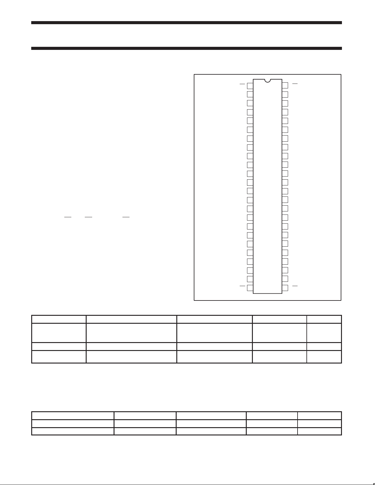
PIN CONFIGURATION
1
1OE
1Y0
2
1Y1
3
GND
4
1Y2
5
1Y3
6
V
7
CC
2Y0
8
2Y1
9
GND
10
11
2Y2
12
2Y3
13
3Y0
14
3Y1
15
GND
16
3Y2
17
3Y3
V
18
CC
4Y0
19
4Y1
20
21
GND
22
4Y2
23
4Y3
24
4OE
74L VC16240A
2OE
48
47
1A0
46
1A1
45
GND
44
1A2
43
1A3
42
V
CC
41
2A0
40
2A1
39
GND
38
2A2
37
2A3
36
3A0
35
3A1
34
GND
33
3A2
32
3A3
31
V
CC
30
4A0
29
4A1
28
GND
27
4A2
26
4A3
25
3OE
SW00041
QUICK REFERENCE DA TA
GND = 0 V; T
SYMBOL
t
PHL/tPLH
C
I
C
PD
NOTES:
is used to determine the dynamic power dissipation (PD in W):
1. C
PD
= CPD x V
P
D
f
= input frequency in MHz; CL = output load capacity in pF;
i
= output frequency in MHz; VCC = supply voltage in V;
f
o
(C
L
= 25 C; tr = tf 2.5 ns
amb
2
x fi + (CL x V
CC
2
x V
x fo) = sum of outputs.
CC
PARAMETER CONDITIONS TYPICAL UNIT
Propagation delay
1An to 1Yn;
2An to 2Yn
CL = 50pF
VCC = 3.3V
2.7 ns
Input capacitance 5.0 pF
Power dissipation capacitance per
buffer
2
x fo) where:
CC
VCC = 3.3V 25 pF
ORDERING INFORMATION
PACKAGES TEMPERATURE RANGE OUTSIDE NORTH AMERICA NORTH AMERICA DWG NUMBER
48-Pin Plastic SSOP Type III –40°C to +85°C 74LVC16240A DL VC16240A DL SOT370-1
48-Pin Plastic TSSOP Type II –40°C to +85°C 74LVC16240A DGG VC16240A DGG SOT362-1
1997 Jul 29 853-2007 18218
2
Philips Semiconductors Product specification
16-bit buffer/line driver; inverting (3-State)
PIN DESCRIPTION
PIN NUMBER SYMBOL NAME AND FUNCTION
1 1OE
2, 3, 5, 6 1Y0 to 1Y3 Data outputs
4, 10, 15, 21,
28, 34, 39, 45
7, 18, 31, 42 V
GND Ground (0V)
CC
8, 9, 11, 12 2Y0 to 2Y3 Data outputs
13, 14, 16, 17 3Y0 to 3Y3 Data outputs
19, 20, 22, 23 4Y0 to 4Y3 Data outputs
24 4OE
25 3OE
30, 29, 27, 26 4A0 to 4A3 Data inputs
36, 35, 33, 32 3A0 to 3A3 Data inputs
41, 40, 38, 37 2A0 to 2A3 Data inputs
47, 46, 44, 43 1A0 to 1A3 Data inputs
48 2OE
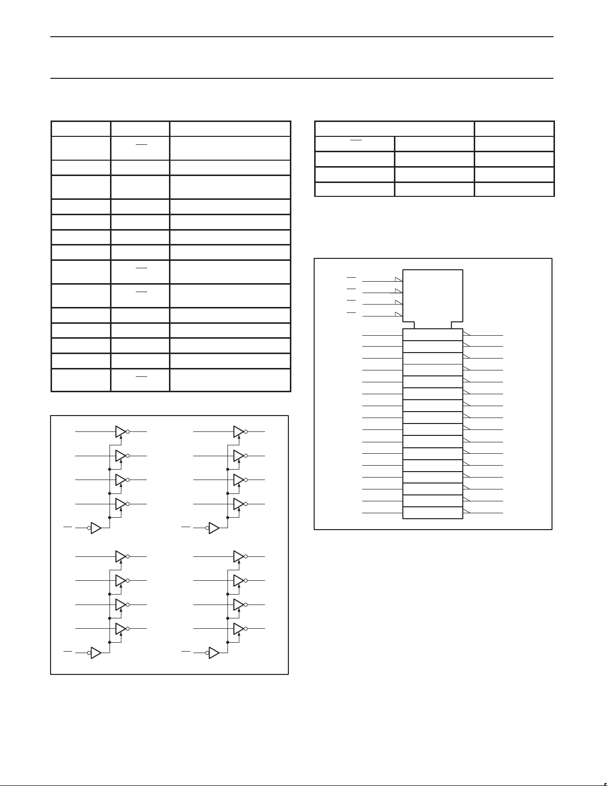
LOGIC SYMBOL
1A0
1A1
1A2
1A3
1OE
47
46
44
43
1
2
3
5
6
Output enable input
(active LOW)
Positive supply voltage
Output enable input
(active LOW)
Output enable input
(active LOW)
Output enable input
(active LOW)
36
3A0
1Y0
35
3A1
1Y1
33
3A2
1Y2
32
3A3
1Y3
25
3OE
13
3Y0
14
3Y1
16
3Y2
17
3Y3
FUNCTION TABLE
INPUTS OUTPUT
nOE nAn nYn
L L H
L H L
H X Z
H = HIGH voltage level
L = LOW voltage level
X = don’t care
Z = high impedance OFF-state
LOGIC SYMBOL (IEEE/IEC)
1OE
2OE
3OE
4OE
1A0
1A1
1A2
1A3
2A0
2A1
2A2
2A3
3A0
3A1
3A2
3A3
4A0
4A1
4A2
4A3
1
48
25
24
47
46
44
43
41
40
38
37
36
35
33
32
30
29
27
26
EN1
EN2
EN3
EN4
74LVC16240A
1 ∇
1
2 ∇1
12
3 ∇1
4 ∇1
13
14
16
17
19
20
22
23
SW00059
2
1Y0
3
1Y1
5
1Y2
6
1Y3
8
2Y0
9
2Y1
11
2Y2
2Y3
3Y0
3Y1
3Y2
3Y3
4Y0
4Y1
4Y2
4Y3
41
2A0
40
2A1
38
2A2
37
2A3
48
2OE
1997 Jul 29
8
2Y0
9
2Y1
11
2Y2
12
2Y3
4A0
4A1
4A2
4A3
4OE
30
29
27
26
24
19
4Y0
20
4Y1
22
4Y2
23
4Y3
SW00042
3
 Loading...