

Philips 74LVC157PW, 74LVC157DB, 74LVC157D, 74LVC157APW, 74LVC157ADB Datasheet
...
74LVC157A
Quad 2-input multiplexer
Product specification
Supercedes data of 1997 Nov 07
IC24 Data Handbook
1998 Jul 29
INTEGRATED CIRCUITS
Philips Semiconductors Product specification
74L VC157AQuad 2-input multiplexer
2
1998 Jul 29 853-1945 19802
FEA TURES
•Wide supply voltage range of 1.2 to 3.6 V
•In accordance with JEDEC standard no. 8-1A
•CMOS lower power consumption
•Direct interface with TTL levels
•5 Volt tolerant inputs, for interfacing with 5 Volt logic
DESCRIPTION
The 74LVC157A is a high-performance, low-power, Si-gate CMOS
device, superior to most advanced CMOS compatible TTL families.
Inputs can be driven from either 3.3V or 5.0V devices. In 3-State
operation, outputs can handle 5V. This feature allows the use of
these devices as translators in a mixed 3.3V/5V environment.
The 74LVC157A is a quad 2-input multiplexer which select 4 bits of
data from two sources under the control of a common data select
input (S). The four outputs present the selected data in the true
(non-inverted) form. The enable input (E
) is active LOW. When E is
HIGH, all of the outputs (1Y to 4Y) are forced LOW regardless of all
other input conditions. Moving the data from two groups of registers
to four common output buses is a common use of the 74LV157. The
state of the common data select input (S) determines the particular
register from which the data comes. It can also be used as function
generator.
The device is useful for implementing highly irregular logic by
generating any four of the 16 different functions of two variables with
one variable common.
The 74LVC157A is the logic implementation of a 4-pole, 2-position
switch, where the position of the switch is determined by the logic
levels applied to S.
QUICK REFERENCE DA TA
GND = 0 V; T
amb
= 25°C; tr = t
f
≤ 2.5 ns
SYMBOL
PARAMETER CONDITIONS TYPICAL UNIT
t
PHL/tPLH
Propagation delay
nl0, nl1, to nY
E
to nY
S to nY
CL = 50 pF;
VCC = 3.3 V
3.1
3.0
3.3
ns
C
I
Input capacitance 5.0 pF
C
PD
Power dissipation capacitance per gate VI = GND to V
CC
1
33 pF
NOTES:
1. C
PD
is used to determine the dynamic power dissipation (PD in µW)
P
D
= CPD × V
CC
2
× fi Σ (CL × V
CC
2
× fo) where:
f
i
= input frequency in MHz; CL = output load capacitance in pF;
f
o
= output frequency in MHz; VCC = supply voltage in V;
Σ (C
L
× V
CC
2
× fo) = sum of the outputs.
ORDERING INFORMATION
PACKAGES TEMPERATURE RANGE OUTSIDE NORTH AMERICA NORTH AMERICA PKG. DWG. #
16-Pin Plastic SO –40°C to +85°C 74LVC157A D 74LVC157A D SOT109-1
16-Pin Plastic SSOP Type II –40°C to +85°C 74LVC157A DB 74LVC157A DB SOT338-1
16-Pin Plastic TSSOP Type I –40°C to +85°C 74LVC157A PW 74LVC157APW DH SOT403-1
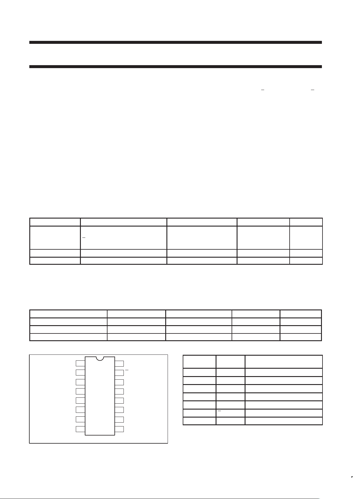
PIN CONFIGURATION
SV00563
1
2
3
4
5
6
S
1I
0
1I
1
1Y
2I
0
2I
1
V
CC
E
4I
0
4I
1
4Y
3I
0
16
15
14
13
12
11
7
8
2Y
GND
3I
1
3Y
10
9
PIN DESCRIPTION
PIN
NUMBER
SYMBOL FUNCTION
1 S Common data select input
2, 5, 11, 14 1l0 to 4l
0
Data inputs from sources 0
3, 6, 10, 13 1l1 to 4l
1
Data inputs from sources 1
4, 7, 9, 12 1Y to 4Y Multiplexer outputs
8 GND Ground (0 V)
15 E Enable input (active LOW)
16 V
CC
Positive supply voltage

Philips Semiconductors Product specification
74LVC157AQuad 2-input multiplexer
1998 Jul 29
3
LOGIC SYMBOL
SV00564
1
S
E
2
1I
0
2I
0
3I
0
4I
0
1I
1
2I
1
3I
1
4I
1
35
4
1Y
6
7
2Y
10
12
4Y
1411
9
3Y
13
15
LOGIC SYMBOL (IEEE/IEC)
SV00565
EN
G1
15
1
7
4
9
12
6
5
3
2
MUX
1
11
10
14
13
1
FUNCTIONAL DIAGRAM
SV00566
E
S
SELECTOR
MULTIPLEXER
OUTPUTS
1I
0
1Y
2Y
3Y
4Y
1I
1
2I
0
2I
1
3I
0
3I
1
4I
0
4I
1
115
7
4
9
12
6
5
2
3
11
10
14
13
FUNCTION T ABLE
INPUTS OUTPUTS
E S nl
0
nl
1
nY
H X X X L
L L L X L
L L H X H
L H X L L
L H X H H
NOTES:
H = HIGH voltage level
L = LOW voltage level
X = don’t care
LOGIC DIAGRAM
SV00581
S
1Y
2Y
3Y
4Y
1I
1
1I
0
2I
1
2I
0
3I
1
3I
0
4I
1
4I
0
E
 Loading...