

Philips 74lvc14a DATASHEETS
INTEGRATED CIRCUITS
74LVC14A
Hex inverting Schmitt-trigger with 5V
tolerant input
Product specification 1998 Apr 28
Philips Semiconductors Product specification
t
gy
L
4
ns
Hex inverting Schmitt-trigger with 5V
tolerant input
FEA TURES
•Wide supply voltage range of: 1.2 V to 3.6 V
•In accordance with JEDEC standard no. 8-1A
•Inputs accept voltages up to 5.5 V
•CMOS low power consumption
•Direct interface with TTL levels
APPLICATIONS
•Wave and pulse shapers for highly noisy environments
•Astable multivibrators
•Monostable multivibrators
QUICK REFERENCE DATA
GND = 0 V; T
SYMBOL
NOTES:
1. C
is used to determine the dynamic power dissipation (PD in µW)
PD
= CPD × V
P
D
fi = input frequency in MHz; CL = output load capacity in pF;
f
= output frequency in MHz; VCC = supply voltage in V;
o
(C
L
2. The condition is V
= 25°C; tr ≤ tf ≤ 2.5 ns
amb
PHL/tPLH
C
I
C
PD
2
× fi (CL × V
CC
2
× V
× fo) = sum of the outputs.
CC
= GND to V
I
PARAMETER CONDITIONS TYPICAL UNIT
Propagation delay CL = 50 pF;
nA to nY
Input capacitance 3.5 pF
Power dissipation capacitance per gate Notes 1 and 2 25 pF
2
× fo) where:
CC
CC.
74L VC14A
DESCRIPTION
The 74LVC14A is a high-performance, low power, low-voltage
Si-gate CMOS device and superior to most advanced CMOS
compatible TTL families.
Inputs can be driven from either 3.3 V or 5 V devices. This feature
allows the use of these devices as translators in a mixed 3.3 V/5 V
environment.
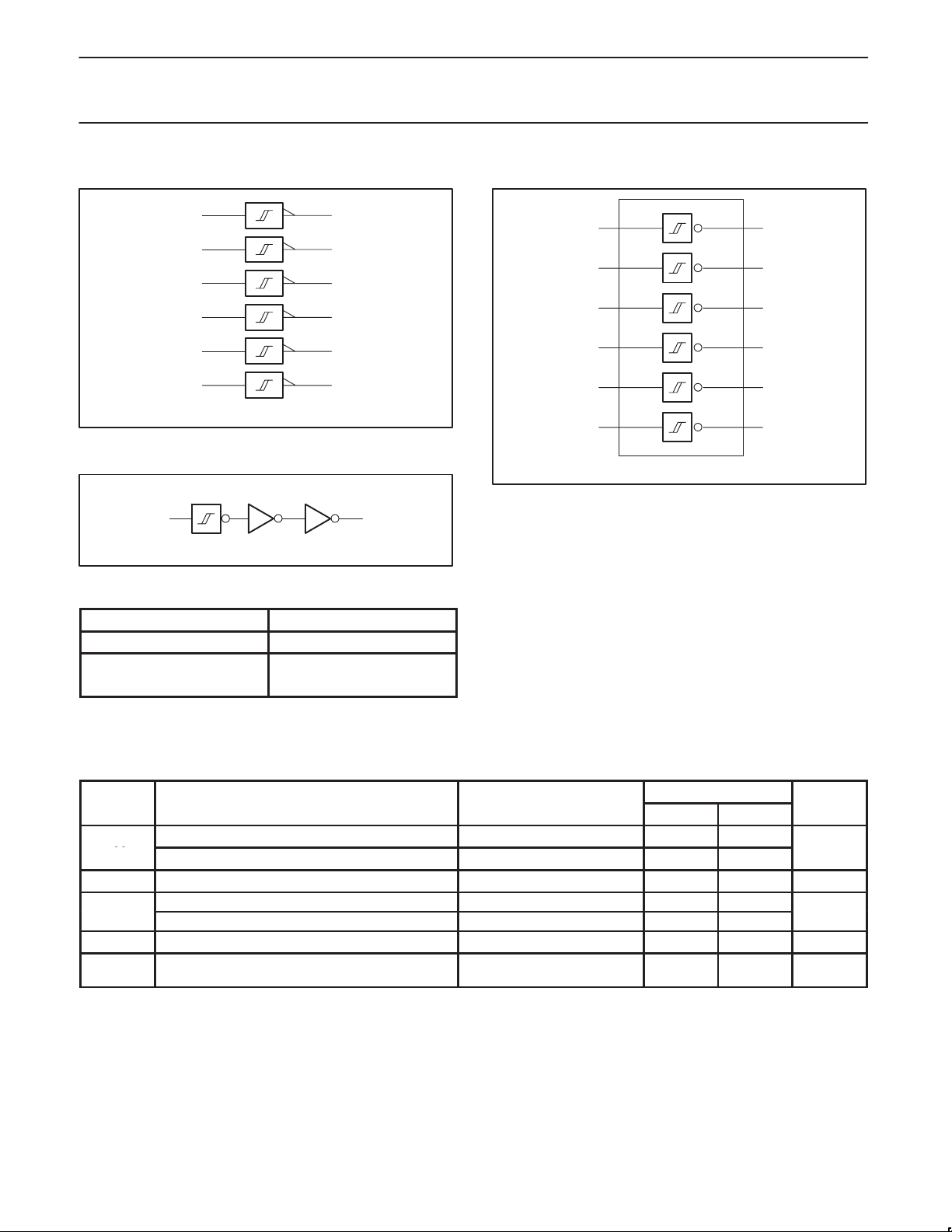
The 74LVC14A provides six inverting buffers with Schmitt-trigger
action. It is capable of transforming slowly changing input signals
into sharply defined, jitter-free output signals.
VCC = 3.3 V
ORDERING INFORMATION
PACKAGES TEMPERATURE RANGE OUTSIDE NORTH AMERICA NORTH AMERICA DWG NUMBER
14-Pin Plastic SO –40°C to +85°C 74LVC14A D 74LVC14A D SOT108-1
14-Pin Plastic SSOP Type II –40°C to +85°C 74LVC14A DB 74LVC14A DB SOT337-1
14-Pin Plastic TSSOP Type I –40°C to +85°C 74LVC14A PW 74LVC14APW DH SOT402-1
PIN CONFIGURATION
1
1A
2
1Y
3
2A
4
2Y
5
3A
6
3Y
GND
7
14
V
13
6A
12
6Y
11
5A
10
5Y
9
4A
8
4Y
SV00396
CC
PIN DESCRIPTION
PIN NUMBER SYMBOL NAME AND FUNCTION
1, 3, 5, 9, 11, 13 1A – 6A Data inputs
2, 4, 6, 8, 10, 12 1Y – 6Y Data outputs
7 GND Ground (0 V)
14 V
CC
Positive supply voltage
1998 Apr 28 853-1907 19308
2
Philips Semiconductors Product specification
SYMBOL
PARAMETER
CONDITIONS
UNIT
V
V
V
V
Hex inverting Schmitt-trigger with 5V
tolerant input
LOGIC SYMBOL (IEEE/IEC)
1
3
5
9
11
13
LOGIC DIAGRAM (ONE SCHMITT-TRIGGER)
AY
2
4
6
8
10
12
SV00425
LOGIC SYMBOL
1A 1Y
1
2A
3
3A 3Y
5
4A 4Y
9
5A 5Y
11
6A
13
74LVC14A
2
4
2Y
6
8
10
12
6Y
SV00424
SV00426
FUNCTION TABLE
INPUT OUTPUT
nA nY
L H
H L
NOTES:
H = HIGH voltage level
L = LOW voltage level
RECOMMENDED OPERA TING CONDITIONS
DC supply voltage (for max. speed performance) 2.7 3.6
CC
DC supply voltage (for low-voltage applications) 1.2 3.6
T
V
amb
tr, t
DC input voltage range 0 5.5 V
I
DC output voltage range; output HIGH or LOW state 0 V
I/O
DC input voltage range; output 3-State 0 5.5
Operating free-air temperature range –40 +85 °C
Input rise and fall times
f
VCC = 1.2 to 2.7V
V
= 2.7 to 3.6V
CC
LIMITS
MIN MAX
CC
0
0
20
10
ns/V
1998 Apr 28
3
 Loading...