

Philips 74LVC139PW, 74LVC139DB, 74LVC139D Datasheet
INTEGRATED CIRCUITS
74LVC139
Dual 2-to-4 line decoder/demultiplexer
Product specification
Supersedes data of 1997 Jun 19
IC24 Data Handbook
1998 Apr 28
Philips Semiconductors Product specification
Address in uts
Out uts (active LOW)
74L VC139Dual 2-to-4 line decoder/demultiplexer
FEA TURES
•Wide supply voltage range of 1.2 to 3.6 V
•In accordance with JEDEC standard no. 8-1A
•Inputs accept voltages up to 5.5 V
•CMOS lower power consumption
•Direct interface with TTL levels
•Demultiplexing capability
•Two independent 2-to-4 decoders
•Multifunction capability
•Active LOW mutually exclusive outputs
•Output drive capability 50 transmission lines at 85°C
QUICK REFERENCE DATA
GND = 0 V; T
SYMBOL
t
NOTES:
is used to determine the dynamic power dissipation (PD in µW)
1. C
PD
P
= CPD × V
D
= input frequency in MHz; CL = output load capacity in pF;
f
i
f
= output frequency in MHz; VCC = supply voltage in V;
o
(C
L
2. The condition is V
= 25°C; tr = tf ≤ 2.5 ns
amb
PHL/tPLH
C
I
C
PD
2
× fi (CL × V
CC
2
× V
× fo) = sum of the outputs.
CC
= GND to V
1
PARAMETER CONDITIONS TYPICAL UNIT
Propagation delay
nA to nYn,
nE to nYn,
Input capacitance 5.0 pF
Power dissipation capacitance per
multiplexer
2
× fo) where:
CC
CC
DESCRIPTION
The 74LVC139 is a low-voltage, low-power, high-performance
Si-gate CMOS device, superior to most advanced CMOS
compatible TTL families.
The 74LVC139 is a dual 2-to-4 line decoder/demultiplexer. This device
has two independent decoders, each accepting two binary weighted
inputs (nA
outputs (nY
When nE is HIGH, every output is forced HIGH. The enable can be
used as the data input for a 1-to-4 demultiplexer application.
CL = 50 pF;
VCC = 3.3 V
VCC = 3.3 V
Notes 1 and 2
and nA1) and providing four mutually exclusive active LOW
0
to nY3). Each decoder has an active LOW input (nE).
0
3.3
3.2
36 pF
ns
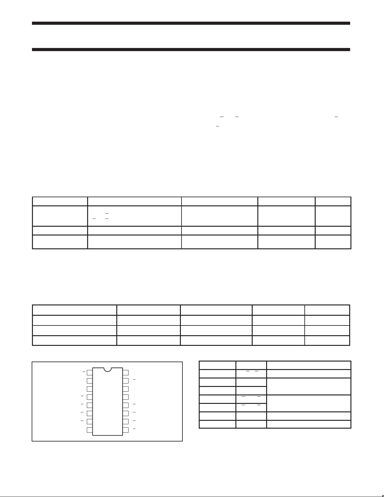
ORDERING INFORMATION
16-Pin Plastic SO –40°C to +85°C 74LVC139 D 74LVC139 D SOT109-1
16-Pin Plastic SSOP Type II –40°C to +85°C 74LVC139 DB 74LVC139 DB SOT338-1
16-Pin Plastic TSSOP Type I –40°C to +85°C 74LVC139 PW 74LVC139PW DH SOT403-1
PIN CONFIGURATION
1998 Apr 28 853-2059 19309
PACKAGES TEMPERATURE RANGE OUTSIDE NORTH AMERICA NORTH AMERICA PKG. DWG. #
PIN DESCRIPTION
PIN NUMBER SYMBOL NAME AND FUNCTION
V
16
CC
15
2E
14
2A
0
13
2A
1
9
2Y
0
10
2Y
1
11
2Y
2
12
2Y
3
SV00530
1, 15 1E, 2E Enable inputs (active LOW)
2, 3 1A0, 1A
14, 13 2A0, 2A
4, 5, 6, 7 1Y0 to 1Y
12, 11, 10, 9 2Y0 to 2Y
1
1
3
3
p
p
8 GND Ground (0 V)
16 V
CC
Positive supply voltage
2
1A
1A
1Y
1Y
1Y
1Y
GND
1
1E
2
0
3
1
4
0
5
1
6
2
7
3
8
Philips Semiconductors Product specification
Dual 2-to-4 line decoder/demultiplexer
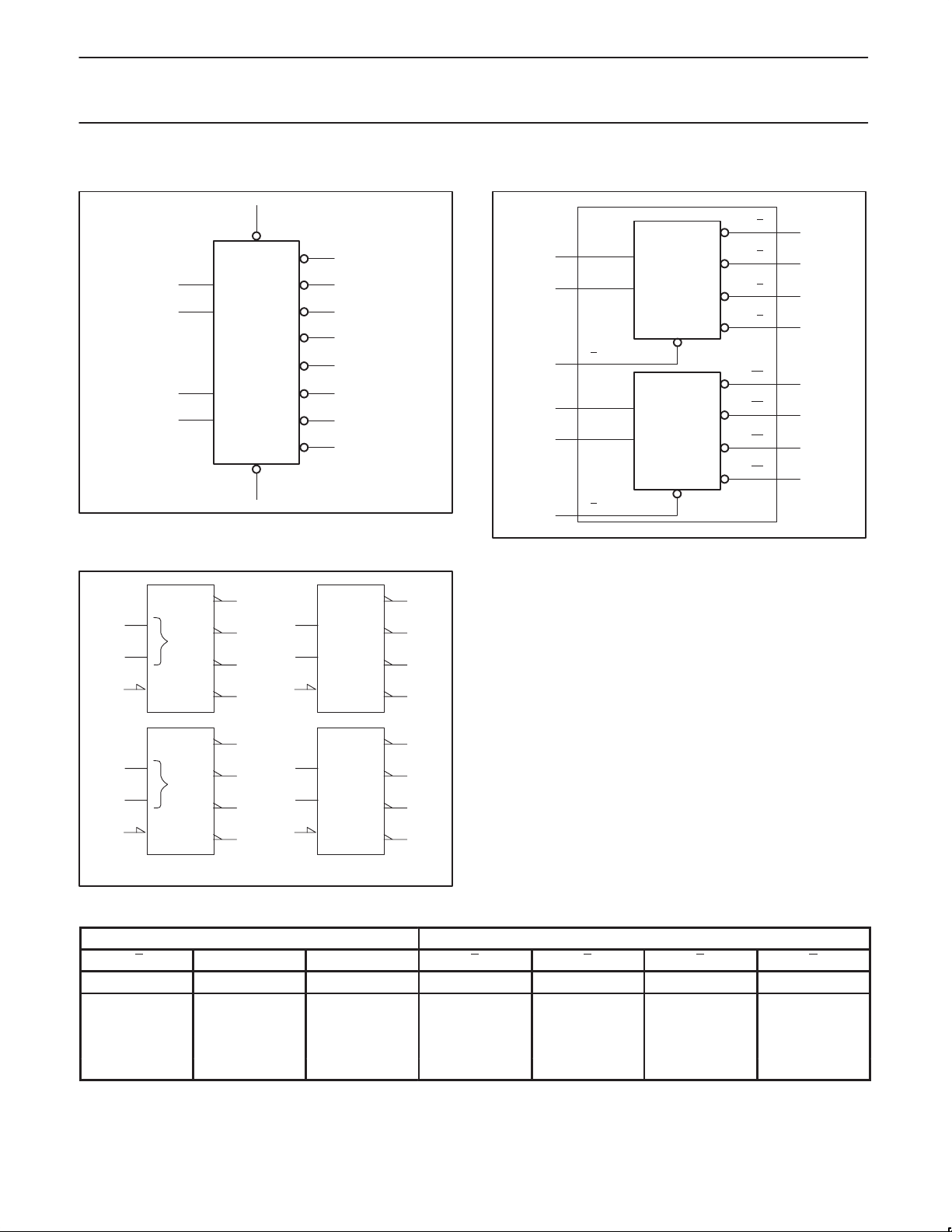
LOGIC DIAGRAM
1
1E
1Y
0
2
3
14
13
1A
1A
2A
2A
1Y
0
1
0
1
1
1Y
2
1Y
3
2Y
0
2Y
1
2Y
2
2Y
3
2E
15
4
5
6
7
12
11
10
9
SV00531
FUNCTIONAL DIAGRAM
1A
2
3
1
14
13
15
o
1A
1
1E
1A
o
2A
1
2E
DECODER
DECODER
74LVC139
1Y
0
4
1Y
1
5
1Y
2
6
1Y
3
7
2Y
0
12
2Y
1
11
2Y
2
10
2Y
3
9
SV00534
LOGIC SYMBOL (IEEE/IEC)
DX X/Y
22
01
G0––
3
12
33
11
DX X/Y
14 14
01
G0––
3
12
13 13
15 15
(a) (b)
44
00
11
55
22
66
33
77
12 12
00
11 11
11
10 10
22
33
99
EN
EN
FUNCTION TABLE
INPUTS OUTPUTS
nE nA
H X X H H H H
L L L L H H H
L H L H L H H
L L H H H L H
L H H H H H L
NOTES:
H = HIGH voltage level
L = LOW voltage level
X = don’t care
0
nA
1
SV00532
nY
0
nY
1
nY
2
nY
3
1998 Apr 28
3
 Loading...