

Philips 74LVC138APW, 74LVC138ADB, 74LVC138AD Datasheet

INTEGRATED CIRCUITS
74LVC138A
3-to-8 line decoder/demultiplexer;
inverting
Product specification 1998 Apr 28
Philips Semiconductors Product specification
74L VC138A3-to-8 line decoder/demultiplexer; inverting
FEA TURES
•Wide supply voltage range of 1.2 to 3.6 V
•In accordance with JEDEC standard no. 8-1A
•Inputs accept voltages up to 5.5 V
•CMOS lower power consumption
•Direct interface with TTL levels
•Demultiplexing capability
•Multiple input enable for easy expansion
•Ideal for memory chip select decoding
•Active LOW mutually exclusive outputs
•Output drive capability 50 transmission lines at 85°C
QUICK REFERENCE DATA
GND = 0 V; T
SYMBOL
t
NOTES:
is used to determine the dynamic power dissipation (PD in µW)
1. C
PD
P
= CPD × V
D
fi = input frequency in MHz; CL = output load capacity in pF;
f
= output frequency in MHz; VCC = supply voltage in V;
o
(C
L
2. The condition is VI = GND to V
= 25°C; tr = tf ≤ 2.5 ns
amb
PHL/tPLH
C
I
C
PD
2
× fi (CL × V
CC
2
× V
× fo) = sum of the outputs.
CC
PARAMETER CONDITIONS TYPICAL UNIT
Propagation delay
An to Yn,
E3 to Yn, En to Yn
Input capacitance 5.0 pF
Power dissipation capacitance per
package
2
× fo) where:
CC
CC
DESCRIPTION
The 74LVC138A is a low-voltage, low-power, high-performance
Si-gate CMOS device, superior to most advanced CMOS
compatible TTL families.
The 74LVC138A accepts three binary weighted address inputs (A
A
, A2) and when enabled, provides 8 mutually exclusive active
1
LOW outputs (Y
The 74LVC138A features three enable inputs: two active LOW (E
and E2) and one active HIGH (E3). Every output will be HIGH unless
E
and E2 are LOW and E3 is HIGH.
1
This multiple enable function allows easy parallel expansion of the
74LV138A to a 1-of-32 (5 lines to 32 lines) decoder with just four
74LV138A ICs and one inverter. The 74LV138A can be used as an
eight output demultiplexer by using one of the active LOW enable
inputs as the data input and the remaining enable inputs as strobes.
Unused enable inputs must be permanently tied to their appropriate
active HIGH or LOW state.
CL = 50 pF;
VCC = 3.3 V
VCC = 3.3 V
Notes 1 and 2
to Y7).
0
3.5
3.5
44 pF
ns
,
0
1
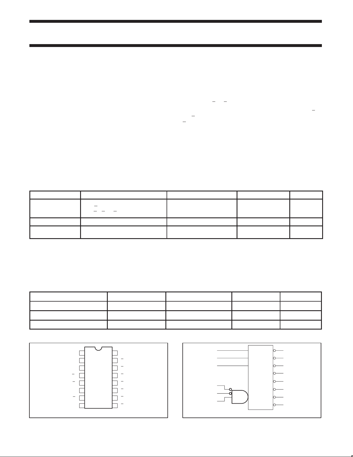
ORDERING INFORMATION
PACKAGES TEMPERATURE RANGE OUTSIDE NORTH AMERICA NORTH AMERICA PKG. DWG. #
16-Pin Plastic SO –40°C to +85°C 74LVC138A D 74LVC138A D SOT109-1
16-Pin Plastic SSOP Type II –40°C to +85°C 74LVC138A DB 74LVC138A DB SOT338-1
16-Pin Plastic TSSOP Type I –40°C to +85°C 74LVC138A PW 74LVC138APW DH SOT403-1
PIN CONFIGURATION
1
A
0
A
2
1
3
A
2
4
E
1
5
E
2
6
E
3
7
Y
7
8
GND
1998 Apr 28 853–1943 19308
V
16
Y
15
Y
14
Y
13
Y
12
Y
11
Y
10
Y
9
SV00553
CC
0
0
0
0
0
0
0
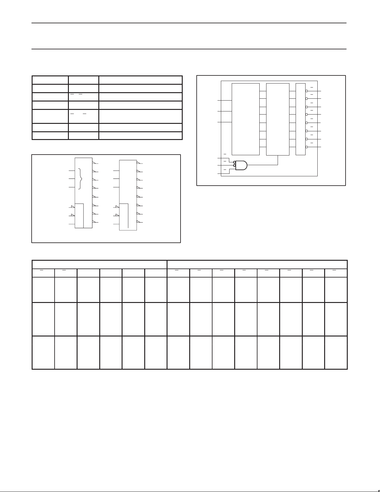
LOGIC DIAGRAM
2
1
2
3
4
5
6
E
1
E
2
E
3
Y
A
0
Y
A
1
Y
A
2
Y
Y
Y
Y
Y
0
1
2
3
4
5
6
7
SV00554
15
14
13
12
11
10
9
7
Philips Semiconductors Product specification
74LVC138A3-to-8 line decoder/demultiplexer; inverting
PIN DESCRIPTION
PIN NUMBER SYMBOL NAME AND FUNCTION
1, 2, 3 A0 to A
4, 5 E1, E
6 E
15, 14, 13, 12,
11, 10, 9, 7
3
Y0 to Y
2
Address inputs
2
Enable inputs (active LOW)
Enable inputs (active HIGH)
Outputs
7
8 GND Ground (0 V)
16 V
CC
Positive supply voltage
LOGIC SYMBOL (IEEE/IEC)
0
0
1
2
3
4
5
6
1
2
2
3
4
5
&
6
7
(a) (b)
15
14
13
12
11
10
9
7
X/YDX
1
1
2
2
4
3
&
4
5
6
0
1
2
3
4
5
6
EN
7
SV00555
15
14
13
12
11
10
9
7
FUNCTIONAL DIAGRAM
A
1
1
A
2
2
3
4
5
6
A
E
E
E
3
1
2
3
3-to-8
DECODER
ENABLE
EXITING
Y
0
Y
1
Y
2
Y
3
Y
4
Y
5
Y
6
Y
7
SV00556
15
14
13
12
11
10
9
7
FUNCTION TABLE
INPUTS OUTPUTS
E
1
H X X X X X H H H H H H H H
X H X X X X H H H H H H H H
X X L X X X H H H H H H H H
L L H L L L L H H H H H H H
L L H H L L H L H H H H H H
L L H L H L H H L H H H H H
L L H H H L H H H L H H H H
L L H L L H H H H H L H H H
L L H H L H H H H H H L H H
L L H L H H H H H H H H L H
L L H H H H H H H H H H H L
NOTES:
H = HIGH voltage level
L = LOW voltage level
X = don’t care
E
2
E
3
A
A
0
1
A
2
Y
0
Y
1
Y
2
Y
3
Y
4
Y
5
Y
6
Y
7
1998 Apr 28
3
 Loading...