

Philips 74lvc126a DATASHEETS
INTEGRATED CIRCUITS
74LVC126A
Quad buffer/line driver with 5-volt tolerant
inputs/outputs (3-State)
Product specification
Supersedes data of 1997 Aug 01
IC24 Data Handbook
1998 Apr 28

Philips Semiconductors Product specification
Quad buffer/line driver with 5-volt tolerant
inputs/outputs (3-state)
FEA TURES
•5-volt tolerant inputs/outputs, for interfacing with 5-volt logic
•Supply voltage range of 1.2V to 3.6V
•Complies with JEDEC standard no. 8-1A
•CMOS low power consumption
•Direct interface with TTL levels
•High impedance when V
QUICK REFERENCE DATA
GND = 0 V; T
SYMBOL
t
NOTES:
is used to determine the dynamic power dissipation (PD in µW)
1. C
PD
P
= CPD × V
D
= input frequency in MHz; CL = output load capacity in pF;
f
i
f
= output frequency in MHz; VCC = supply voltage in V;
o
(C
L
2. The condition is V
= 25°C; tr = tf ≤ 2.5 ns
amb
PHL/tPLH
C
I
C
PD
2
× fi (CL × V
CC
2
× V
× fo) = sum of the outputs.
CC
= 0V
CC
PARAMETER CONDITIONS TYPICAL UNIT
Propagation delay
nA to nY
CL = 50 pF;
VCC = 3.3 V
Input capacitance 5.0 pF
Power dissipation capacitance per buffer VCC = 3.3 V 20 pF
2
× fo) where:
CC
= GND to V
I
CC
74L VC126A
DESCRIPTION
The 74LVC126A is a high performance, low-power, low-voltage
Si-gate CMOS device and superior to most advanced CMOS
compatible TTL families.
Inputs can be driven from either 3.3V or 5.0V devices. In 3-state
operation, outputs can handle 5V .
The 74LVC126A consists of four non-inverting buffers/line drivers
with 3-state outputs. The 3-state outputs (nY) are controlled by the
output enable input (nOE). A LOW at nOE causes the outputs to
assume a high impedance OFF-state.
3.0 ns
ORDERING INFORMATION
PACKAGES TEMPERATURE RANGE OUTSIDE NORTH AMERICA NORTH AMERICA PKG. DWG. #
14-Pin Plastic SO –40°C to +125°C 74LVC126A D 74LVC126A D SOT108-1
14-Pin Plastic SSOP Type II –40°C to +125°C 74LVC126A DB 74LVC126A DB SOT337-1
14-Pin Plastic TSSOP Type I –40°C to +125°C 74LVC126A PW 74LVC126APW DH SOT402-1
PIN CONFIGURATION
1
1OE
2
1A
3
1Y
4
2OE
5
2A
6
2Y
GND
7
14
13
12
11
10
9
8
SV00483
V
4OE
4A
4Y
3OE
3A
3Y
CC
PIN DESCRIPTION
PIN
NUMBER
1, 4, 10, 13 1OE – 4OE Data enable inputs (active HIGH)
2, 5, 9, 12 1A – 4A Data inputs
3, 6, 8, 11 1Y – 4Y Data Outputs
7 GND Ground (0 V)
14 V
SYMBOL NAME AND FUNCTION
CC
Positive supply voltage
1998 Apr 28 853-2009 19310
2
Philips Semiconductors Product specification
SYMBOL
PARAMETER
CONDITIONS
UNIT
V
V
V
V
Quad buffer/line driver with 5-volt tolerant
inputs/outputs (3-state)
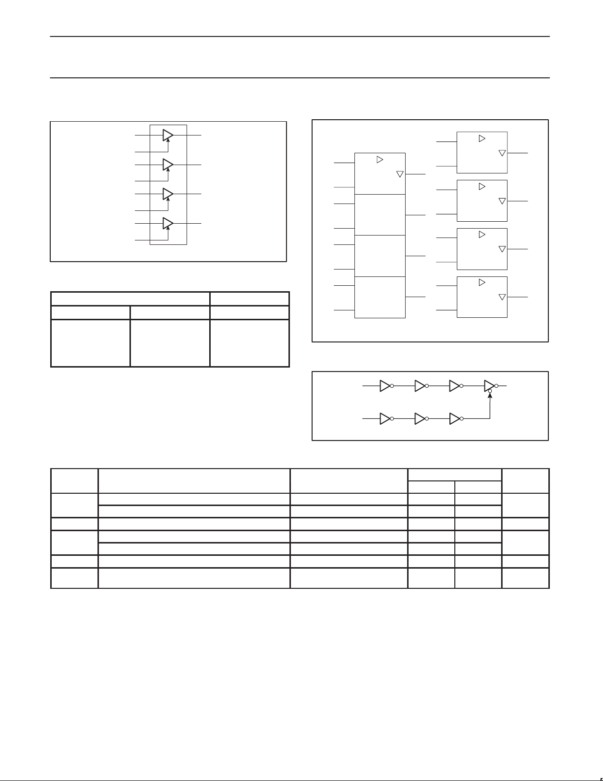
LOGIC SYMBOL
3
1A
1OE
2A
2OE
3A
3OE
4A
4OE
1Y
2Y
3Y
4Y
SV00484
6
8
11
2
1
5
4
9
10
12
13
FUNCTION TABLE
INPUTS OUTPUT
nOE nA nY
H L L
H H H
L X Z
NOTES:
H = HIGH voltage level
L = LOW voltage level
X = don’t care
Z = high impedance OFF-state
LOGIC SYMBOL (IEEE/IEC)
2
1
EN1
5
4
9
10
12
13
1
(a) (b)
3
6
8
11
LOGIC DIAGRAM
nOE
74LVC126A
2
3
1
EN
5
6
4
EN
9
8
10
EN
12
11
13
EN
SV00485
nYnA
RECOMMENDED OPERA TING CONDITIONS
DC supply voltage (for max. speed performance) 2.7 3.6
CC
DC supply voltage (for low-voltage applications) 1.2 3.6
T
V
amb
tr, t
DC input voltage range 0 5.5 V
I
DC output voltage range; output HIGH or LOW state 0 V
O
DC output voltage range; output 3-State 0 5.5
Operating ambient temperature range in free-air –40 +85 °C
Input rise and fall times
f
VCC = 1.2 to 2.7V
VCC = 2.7 to 3.6V
LIMITS
MIN MAX
CC
0
0
20
10
SV00486
ns/V
1998 Apr 28
3
 Loading...