

Philips 74LVC11PW, 74LVC11DB, 74LVC11D Datasheet
INTEGRATED CIRCUITS
74LVC11
Triple 3-input AND gate
Product specification 1998 Apr 28
Philips Semiconductors Product specification
Triple 3-input AND gate
FEA TURES
•Wide supply voltage range of 1.2 V to 3.6 V
•In accordance with JEDEC standard no. 8-1A.
•Inputs accept voltages up to 5.5 V
•CMOS low power consumption
•Direct interface with TTL levels
•Output capability: standard
•I
category: SSI
CC
QUICK REFERENCE DATA
GND = 0 V; T
SYMBOL
t
NOTES:
1. C
is used to determine the dynamic power dissipation (PD in µW)
PD
= CPD × V
P
D
= input frequency in MHz; CL = output load capacity in pF;
f
i
f
= output frequency in MHz; VCC = supply voltage in V;
o
(C
L
2. The condition is V
= 25°C; tr = tf 2.5 ns
amb
PHL/tPLH
C
I
C
PD
2
× fi (CL × V
CC
2
× V
× fo) = sum of the outputs.
CC
= GND to V
I
PARAMETER CONDITIONS TYPICAL UNIT
Propagation delay
nA, nB, nC to nY
Input capacitance 5.0 pF
Power dissipation capacitance per gate Notes 1 and 2 26 pF
2
× fo) where:
CC
CC.
74L VC11
DESCRIPTION
The 74LVC11 is a high-performance, low power, low-voltage Si-gate
CMOS device and superior to most advanced CMOS compatible
TTL families.
The 74LVC11 provides the 3-input AND function.
CL = 50 pF;
VCC = 3.3 V
3.7 ns
ORDERING INFORMATION
PACKAGES TEMPERATURE RANGE OUTSIDE NORTH AMERICA NORTH AMERICA DWG NUMBER
14-Pin Plastic SO –40°C to +85°C 74LVC11 D 74LVC11 D SOT108-1
14-Pin Plastic SSOP Type II –40°C to +85°C 74LVC11 DB 74LVC11 DB SOT337-1
14-Pin Plastic TSSOP Type I –40°C to +85°C 74LVC11 PW 74LVC11PW DH SOT402-1
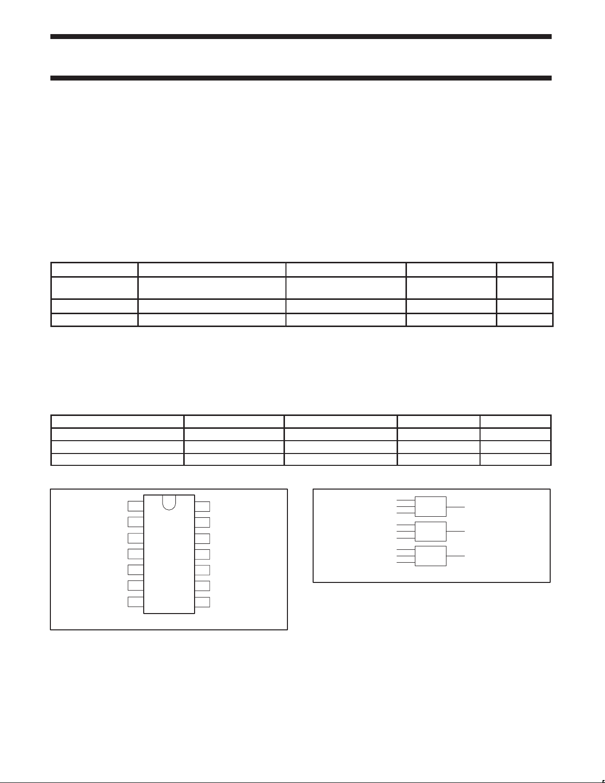
PIN CONFIGURATION
1
1A
2
1B
3
2A
4
2B
5
2C
6
2Y
7
GND
14
13
12
11
10
9
8
SV00416
V
CC
1C
1Y
3C
3B
3A
3Y
LOGIC SYMBOL (IEEE/IEC)
1
2
13
3
4
5
9
10
11
&
&
&
12
6
8
SV00439
1998 Apr 28 853-2060 19308
2
Philips Semiconductors Product specification
SYMBOL
PARAMETER
CONDITIONS
UNIT
Triple 3-input AND gate
PIN DESCRIPTION
PIN
NUMBER
1, 3, 9 1A – 3A Data inputs
2, 4, 10 1B – 3B Data inputs
7 GND Ground (0 V)
12, 6, 8 1Y – 3Y Data outputs
13, 5, 11 1C – 3C Data inputs
14 V
LOGIC SYMBOL
SYMBOL NAME AND FUNCTION
CC
Positive supply voltage
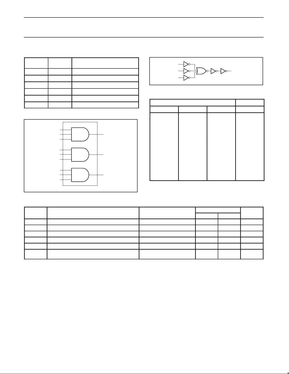
1A131
1B2
1C
3
2B4
2C2A5
3A119
3B10
3C
2Y
3Y
SV00438
74LVC11
LOGIC DIAGRAM (ONE GATE)
A
B
C
FUNCTION TABLE
INPUTS OUTPUTS
nA nB nC nY
L L L L
L L H L
121Y
6
8
L H L L
L H H L
H L L L
H L H L
H H L L
H H H H
NOTES:
H = HIGH voltage level
L = LOW voltage level
Y
SV00421
RECOMMENDED OPERATING CONDITIONS
V
V
T
V
V
amb
tr, t
DC supply voltage (for max. speed performance) 2.7 3.6 V
CC
DC supply voltage (for low-voltage applications) 1.2 3.6 V
CC
DC input voltage range 0 5.5 V
I
DC output voltage range 0 V
O
Operating free-air temperature range –40 +85 °C
Input rise and fall times
f
VCC = 1.2 to 2.7V
VCC = 2.7 to 3.6V
LIMITS
MIN MAX
CC
0
0
20
10
V
ns/V
1998 Apr 28
3
 Loading...