

Philips 74LVC109PW, 74LVC109DB, 74LVC109D Datasheet
INTEGRATED CIRCUITS
74LVC109
Dual JK
flip-flop with set and reset;
positive-edge trigger
Product specification
Supersedes data of 1997 Mar 18
IC24 Data Handbook
1998 Apr 28
Philips Semiconductors Product specification
74L VC109Dual JK flip-flop with set and reset; positive-edge trigger
FEA TURES
•Wide supply voltage range of 1.2 to 3.6 V
•In accordance with JEDEC standard no. 8-1A.
•Inputs accept voltages up to 5.5 V
•CMOS low power consumption
•Direct interface with TTL levels
•Output capability: standard
•I
category: flip-flops
CC
QUICK REFERENCE DATA
GND = 0 V; T
= 25°C; tr = t
amb
SYMBOL
Propagation delay
t
PHL/tPLH
nCP to nQ, nQ
nSD to nQ, nQ
nRD to nQ, nQ
f
max
C
C
I
PD
Maximum clock frequency 250 MHz
Input capacitance 5.0 pF
Power dissipation capacitance per flip-flop VI = GND to V
NOTE:
is used to determine the dynamic power dissipation (PD in µW)
1. C
PD
= CPD × V
P
D
f
= input frequency in MHz; CL = output load capacity in pF;
i
= output frequency in MHz; VCC = supply voltage in V;
f
o
Σ (C
× V
L
2
× fi Σ (CL × V
CC
2
× fo) = sum of the outputs.
CC
≤ 2.5 ns
f
PARAMETER CONDITIONS TYPICAL UNIT
2
× fo) where:
CC
CL = 50 pF;
VCC = 3.3 V
DESCRIPTION
The 74LVC109 is a low-voltage Si-gate CMOS device that is pin and
function compatible with 74HC/HCT109.
The 74LVC109 is a dual positive-edge triggered JK
featuring individual J, K
) inputs; also complementary Q and Q outputs.
(R
D
inputs, clock (CP) inputs, set (SD) and reset
The set and reset are asynchronous active LOW inputs and operate
independently of the clock input.
The J and K
inputs control the state changes of the flip-flops as
described in the mode select function table. The J and K
be stable one set-up time prior to the LOW-to-HIGH clock transition
for predictable operation. The JK design allows operation as a
D-type flip-flop by tying the J and K
inputs together.
Schmitt-trigger action in the clock input makes the circuit highly
tolerant to slower clock rise and fall times.
4.0
4.5
4.5
CC
1
27 pF
-type flip-flop
inputs must
ns
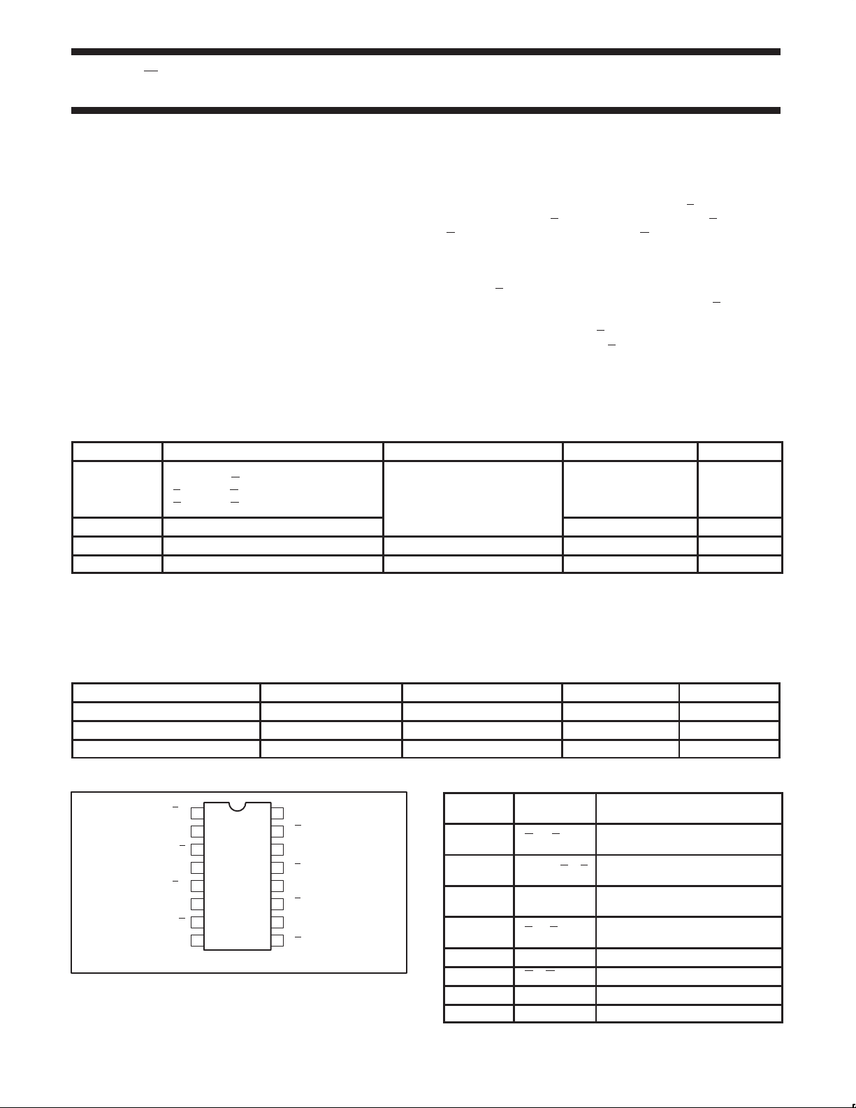
ORDERING INFORMATION
PACKAGES TEMPERATURE RANGE OUTSIDE NORTH AMERICA NORTH AMERICA PKG. DWG. #
16-Pin Plastic SO –40°C to +85°C 74LVC109 D 74LVC109 D SOT109-1
16-Pin Plastic SSOP Type II –40°C to +85°C 74LVC109 DB 74LVC109 DB SOT338-1
16-Pin Plastic TSSOP Type I –40°C to +85°C 74LVC109 PW 74LVC109PW DH SOT403-1
PIN CONFIGURATION
1R
1
D
1J
2
1K
3
1CP
4
1S
5
D
6
1Q
7
1Q
GND
1998 Apr 28 853–1947 19308
16
15
14
13
12
11
10
98
SV00517
V
2R
2J
2K
2CP
2S
2Q
2Q
CC
D
D
PIN DESCRIPTION
PIN
NUMBER
1, 15 1RD, 2R
2, 14, 3, 13 1J, 2J, 1K, 2K
4, 12 1CP, 2CP
5, 11 1S
6, 10 1Q, 2Q True flip-flop outputs
7, 9 1Q, 2Q Complement flip-flop outputs
8 GND Ground (O V)
16 V
2
SYMBOL FUNCTION
Asynchronous reset input
D
(active LOW)
Synchronous inputs;
flip-flops 1 and 2
Clock input
(LOW-to-HIGH, edge-triggered)
Asynchronous set inputs
(active LOW)
Positive supply voltage
CC
2S
D,
D
Philips Semiconductors Product specification
Dual JK
flip-flop with set and reset; positive-edge trigger
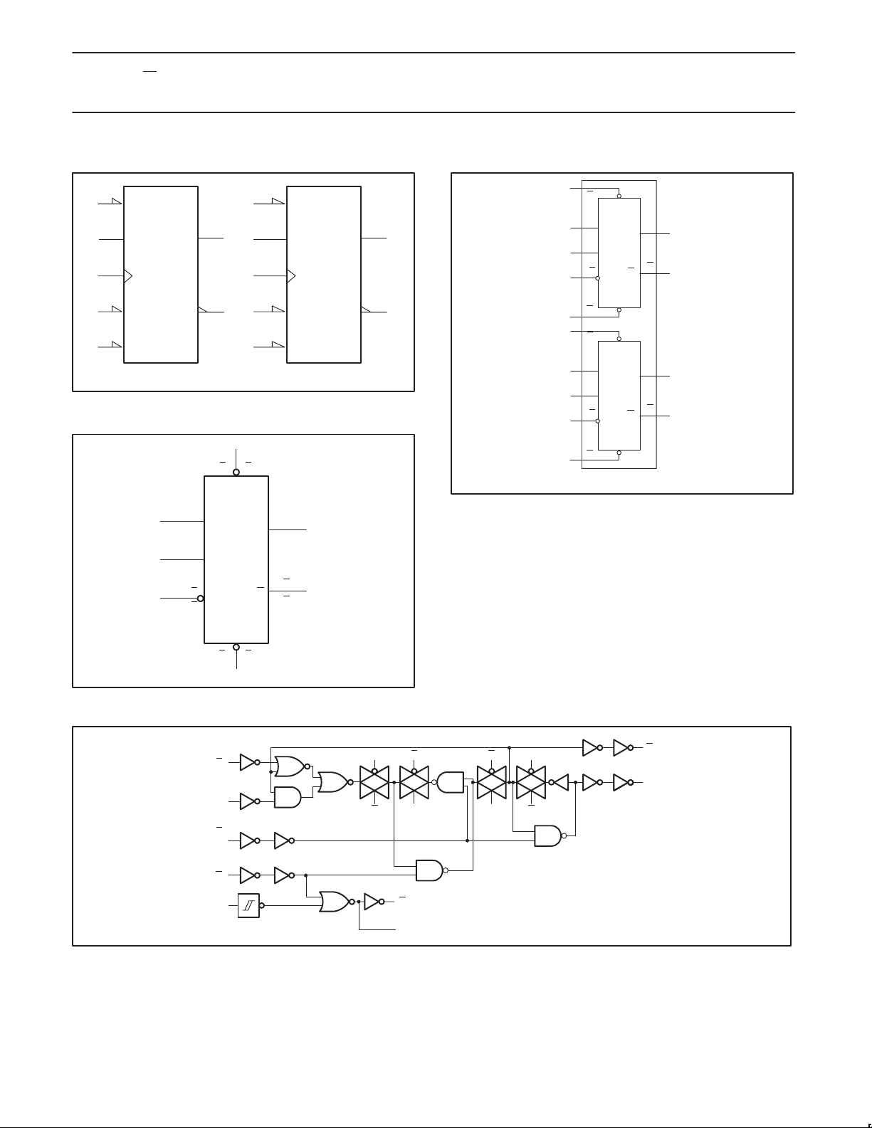
LOGIC SYMBOL (IEEE/IEC)
5
S
2
1J
4
C1
3
1K
1
R
(a) (b)
610
79
LOGIC SYMBOL
11
5
1S
2S
D
74LVC109
FUNCTIONAL DIAGRAM
11
S
14
1J
12
13
15
D
C1
1K
R
SV00519
5
1S
D
S
D
1J
2
1CP
4
1K
3
1R
D
1
11
2S
D
2J
14
2CP
12
2K
13
2R
15
D
J
CP
K
J
K
CP
R
S
R
Q
FF1
Q
D
D
Q
FF2
Q
D
1Q
1Q
2Q
10
2Q
SV00520
6
7
9
14 2J
4 1CP
12 2CP
13 2K
LOGIC DIAGRAM
2 1J
3 1K
J
CP
K
CP
1Q 6
Q
2Q 10
7
1Q
Q
2Q
9
2R
1R
D
D
15
1
SV00518
C
K
J
S
R
C
C
C
C
C
C
C
C
Q
Q
1998 Apr 28
C
SV00521
3
 Loading...