

Philips 74LVC07A Datasheet

INTEGRATED CIRCUITS
DATA SH EET
74LVC07A
Hex buffer with open-drain outputs
Product specification
File under Integrated Circuits, IC24
2000 Mar 07
Philips Semiconductors Product specification
Hex buffer with open-drain outputs 74LVC07A
FEATURES
• 5 V tolerant inputs and outputs (open drain) for
interfacing with 5 V logic
• Wide supply voltage range from 1.65 to 5.5 V
• CMOS low power consumption
• Direct interface with TTL levels
• Inputs accept voltages up to 5 V
• Complies with JEDEC standard no. 8-1A.
DESCRIPTION
The 74LVC07A is a high-performance, low-power,
low-voltage, Si-gate CMOS device, superior to most
advanced CMOS compatible TTL families. Inputs can be
driven from either 3.3 or 5 V devices. This feature allows
the use of these devices as translators in a mixed
3.3 to 5 V environment.
The 74LVC07A provides six non-inverting buffers.
The outputs ofthe 74LVC07A devices are open drain and
can be connected to other open-drain outputs to
implement active-LOW wired-OR or active-HIGH
wired-AND functions.
QUICK REFERENCE DATA
GND = 0 V; T
=25°C; tr=tf≤2.5 ns.
amb
SYMBOL PARAMETER CONDITIONS TYP. UNIT
t
PLZ/tPZL
C
I
C
PD
propagation delay nA to nY CL= 50 pF; VCC= 3.3 V 2.2 ns
input capacitance 5.0 pF
power dissipation capacitance per gate VI= GND to VCC; note 1 6.0 pF
Note
1. C
is used to determine the dynamic power dissipation (PDin µW).
PD
PD=CPD× V
2
× fi+ Σ (CL× V
CC
2
× fo) where:
CC
fi= input frequency in MHz;
fo= output frequency in MHz;
CL= output load capacitance in pF;
= supply voltage in Volts;
V
CC
Σ (CL× V
2
× fo) = sum of the outputs.
CC
FUNCTION TABLE
See note 1.
INPUT OUTPUT
nA nY
LL
HZ
Note
1. H = HIGH voltage level;
L = LOW voltage level;
Z = high impedance OFF-state.
2000 Mar 07 2
Philips Semiconductors Product specification
Hex buffer with open-drain outputs 74LVC07A
ORDERING INFORMATION
TYPE NUMBER
PACKAGES
TEMPERATURE RANGE PINS PACKAGE MATERIAL CODE
74LVC07AD −40 to +85 °C 14 SO plastic SOT108-1
74LVC07APW 14 TSSOP plastic SOT402-1
PINNING
PIN SYMBOL DESCRIPTION
1, 3, 5, 9, 11 and 13 1A to 6A data inputs
2, 4, 6, 8, 10 and 12 1Y to 6Y data outputs
7 GND ground (0 V)
14 V
handbook, halfpage
1A
1Y
2A
2Y
3A
3Y
GND
1
2
3
4
07
5
6
7
CC
MNA531
14
V
CC
13
6A
12
6Y
11
5A
10
5Y
9
4A
8
4Y
DC supply voltage
handbook, halfpage
211A 1Y
432A 2Y
653A 3Y
894A 4Y
1011 5A 5Y
1213 6A 6Y
Fig.1 Pin configuration.
2000 Mar 07 3
MNA535
Fig.2 Logic symbol.
Philips Semiconductors Product specification
Hex buffer with open-drain outputs 74LVC07A
handbook, halfpage
1A
2A
3A
4A
5A
6A
1
3
5
9
11
13
1
1
1
1
1
1
MNA534
2
1Y
4
2Y
6
3Y
8
4Y
10
5Y
12
6Y
handbook, halfpage
A
MNA533
Y
GND
Fig.3 IEC logic symbol. Fig.4 Logic diagram (one gate).
2000 Mar 07 4
Philips Semiconductors Product specification
Hex buffer with open-drain outputs 74LVC07A
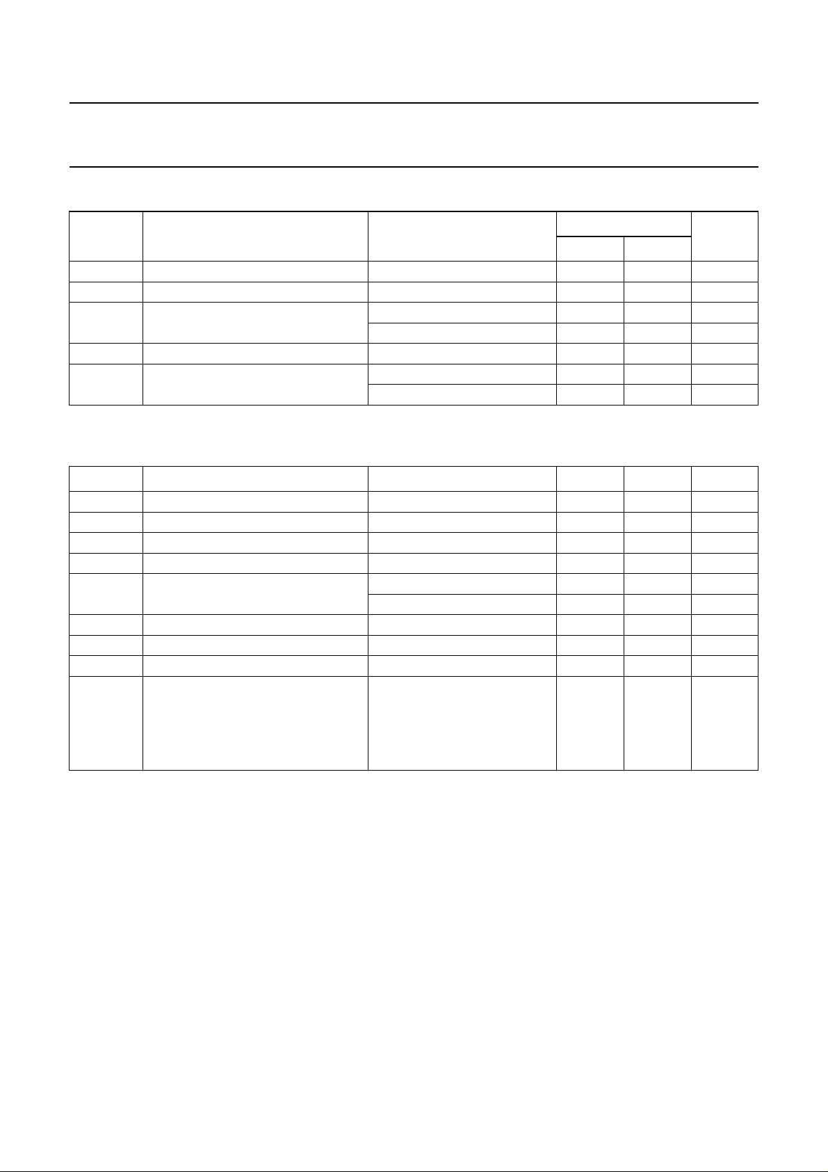
RECOMMENDED OPERATING CONDITIONS
SYMBOL PARAMETER CONDITIONS
UNIT
MIN. MAX.
LIMITS
V
CC
V
I
V
O
DC supply voltage 1.65 5.5 V
DC input voltage 0 5.5 V
DC output voltage active mode 0 V
CC
V
high-impedance mode 0 5.5 V
T
amb
t
, t
r
f
operating ambient temperature −40 +85 °C
input rise and fall ratios VCC= 1.65 to 2.7 V 0 20 ns/V
V
= 2.7 to 5.5 V 0 10 ns/V
CC
LIMITING VALUES
In accordance with the Absolute Maximum Rating System (IEC 60134); voltages are referenced to GND (ground = 0 V).
SYMBOL PARAMETER CONDITIONS MIN. MAX. UNIT
V
CC
I
IK
V
I
I
OK
V
O
DC supply voltage −0.5 +6.5 V
DC input diode current VI<0 −−50 mA
DC input voltage note 1 −0.5 +6.5 V
DC output clamping diode current VO<0 −−50 mA
DC output voltage active mode; note 1 −0.5 VCC+ 0.5 V
high-impedance mode; note 1 −0.5 +6.5 V
I
O
, I
I
CC
GND
T
stg
P
tot
DC output sink current VO=0toV
CC
− 50 mA
DC VCC or GND current −±100 mA
storage temperature −65 +150 °C
power dissipation per package
SO package above 70 °C derate linearly
− 500 mW
with 8 mW/K
TSSOP package above 60 °C derate linearly
− 500 mW
with 5.5 mW/K
Note
1. The input and output voltage ratings may be exceeded if the input and output current ratings are observed.
2000 Mar 07 5
 Loading...