

Philips 74LVC04APW, 74LVC04ADB, 74LVC04DB, 74LVC04D Datasheet
74LVC04A
Hex inverter
Product specification
Supersedes data of 1997 Mar 28
IC24 Data Handbook
1997 Jun 30
INTEGRATED CIRCUITS
Philips Semiconductors Product specification
74L VC04A
Hex inverter
2
1997 Jun 30 853-1953 18162
FEA TURES
•Wide supply range of 1.2V to 3.6V
•Complies with JEDEC standard no. 8-1A
•Inputs accept voltages up to 5.5V
•CMOS low power consumption
•Direct interface with TTL levels
•5-volt tolerant inputs, for interfacing with 5-volt logic
DESCRIPTION
The 74LVC04A is a high-performance, low-power, low-voltage,
Si-gate CMOS device and superior to most advanced CMOS
compatible TTL families.
Inputs can be driven from either 3.3 V or 5 V devices. This feature
allows the use of these devices as translators in a mixed 3.3 V/5 V
environment.
The 74LVC04A provides six inverting buffers.
QUICK REFERENCE DA TA
GND = 0 V; T
amb
= 25°C; tr = tf 2.5 ns
SYMBOL
PARAMETER CONDITIONS TYPICAL UNIT
t
PHL/tPLH
Propagation delay
nA to nY
CL = 50 pF;
VCC = 3.3 V
2.5 ns
C
I
Input capacitance 5.0 pF
C
PD
Power dissipation capacitance per gate Notes 1 and 2 25 pF
NOTES:
1. C
PD
is used to determine the dynamic power dissipation (PD in µW)
P
D
= CPD V
CC
2
x fi (CL V
CC
2
fo) where:
f
i
= input frequency in MHz; CL = output load capacity in pF;
f
o
= output frequency in MHz; VCC = supply voltage in V;
(C
L
V
CC
2
fo) = sum of the outputs.
2. The condition is V
I
= GND to V
CC.
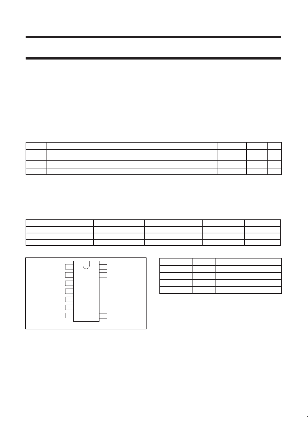
ORDERING INFORMATION
PACKAGES TEMPERATURE RANGE OUTSIDE NORTH AMERICA NORTH AMERICA DWG NUMBER
14-Pin Plastic SO –40°C to +85°C 74LVC04A D 74LVC04A D SOT108-1
14-Pin Plastic SSOP Type II –40°C to +85°C 74LVC04A DB 74LVC04A DB SOT337-1
14-Pin Plastic TSSOP Type I –40°C to +85°C 74LVC04A PW 74LVC04APW DH SOT402-1
PIN CONFIGURATION
1
2
3
4
5
6
7
1A
1Y
2A
2Y
3A
3Y
GND
V
CC
6A
6Y
5A
5Y
4A
4Y
14
13
12
11
10
9
8
SV00396
PIN DESCRIPTION
PIN NUMBER SYMBOL NAME AND FUNCTION
1, 3, 5, 9, 11, 13 1A to 6A Data inputs
2, 4, 6, 8, 10, 12 1Y to 6Y Data outputs
7 GND Ground (0 V)
14 V
CC
Positive supply voltage
Philips Semiconductors Product specification
74LVC04A
Hex inverter
1997 Jun 30
3
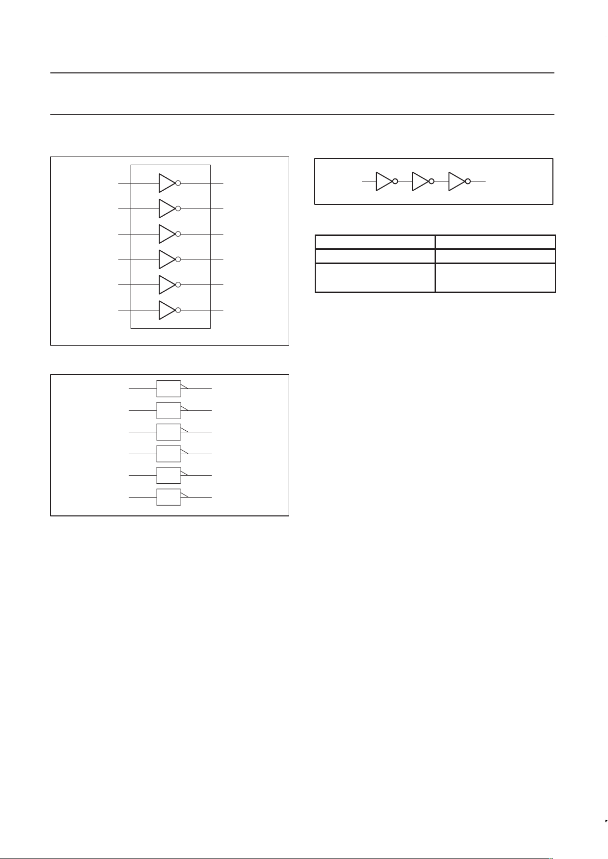
LOGIC SYMBOL
1A 1Y
2A
2Y
3A 3Y
4A 4Y
5A 5Y
6A
6Y
1
3
5
9
11
13
2
4
6
8
10
12
SV00397
LOGIC SYMBOL (IEEE/IEC)
12
34
56
98
11 10
13 12
1
1
1
1
1
1
SV00398
LOGIC DIAGRAM (ONE GA TE)
AY
SV00399
FUNCTION T ABLE
INPUTS OUTPUTS
nA nY
L H
H L
NOTES:
H = HIGH voltage level
L = LOW voltage level
 Loading...