

Philips 74LV74PW, 74LV74N, 74LV74DB, 74LV74D Datasheet
INTEGRATED CIRCUITS
74LV74
Dual D-type flip-flop with set and reset;
positive-edge trigger
Product specification
Supersedes data of 1996 Nov 07
IC24 Data Handbook
1998 Apr 20
Philips Semiconductors Product specification
Dual D-type flip-flop with set and reset;
positive edge-trigger
FEA TURES
•Wide operating voltage: 1.0 to 5.5V
•Optimized for Low Voltage applications: 1.0 to 3.6V
•Accepts TTL input levels between V
•Typical V
T
amb
•Typical V
T
amb
(output ground bounce) 0.8V @ VCC = 3.3V,
OLP
= 25°C
(output VOH undershoot) 2V @ VCC = 3.3V,
OHV
= 25°C
•Output capability: standard
•I
category: flip-flops
CC
QUICK REFERENCE DATA
GND = 0V; T
SYMBOL
t
PHL/tPLH
f
max
C
I
C
PD
NOTES:
1. C
is used to determine the dynamic power dissipation (PD in µW)
PD
= CPD V
P
D
= input frequency in MHz; CL = output load capacitance in pF;
f
i
f
= output frequency in MHz; VCC = supply voltage in V;
o
(C
2. The condition is V
= 25°C; tr =tf 2.5 ns
amb
CC
2
V
L
fo) = sum of the outputs.
CC
Propagation delay
nCP to nQ, nQ
nSD to nQ, nQ
nRD to nQ, nQ
Maximum clock frequency
Input capacitance 3.5 pF
Power dissipation capacitance per flip-flop Notes 1 and 2 24 pF
2
x fi (CL V
= GND to V
I
= 2.7V and VCC = 3.6V
CC
PARAMETER CONDITIONS TYPICAL UNIT
CL = 15pF
V
CC
CL = 15pF
VCC = 3.3V
2
fo) where:
CC
CC
74L V74
DESCRIPTION
The 74LV74 is a low-voltage Si-gate CMOS device and is pin and
function compatible with 74HC/HCT74.
The 74LV74 is a dual positive edge triggered, D-type flip-flop with
individual data (D) inputs, clock (CP) inputs, set (S
inputs; also complementary Q and Q
The set and reset are asynchronous active LOW inputs and operate
independently of the clock input. Information on the data input is
transferred to the Q output on the LOW-to-HIGH transition of the
clock pulse. The D inputs must be stable one set-up time prior to the
LOW-to-HIGH clock transition, for predictable operation.
Schmitt-trigger action in the clock input makes the circuit highly
tolerant to slower clock rise and fall times.
= 3.3V
outputs.
11
14
14
76 MHz
) and (RD)
D
ns
ORDERING INFORMATION
PACKAGES TEMPERATURE RANGE OUTSIDE NORTH AMERICA NORTH AMERICA PKG. DWG. #
14-Pin Plastic DIL –40°C to +125°C 74L V74 N 74LV74 N SOT27-1
14-Pin Plastic SO –40°C to +125°C 74L V74 D 74LV74 D SOT108-1
14-Pin Plastic SSOP Type II –40°C to +125°C 74LV74 DB 74LV74 DB SOT337-1
14-Pin Plastic TSSOP Type I –40°C to +125°C 74L V74 PW 74LV74PW DH SOT402-1
PIN DESCRIPTION
PIN
NUMBER
1, 13 1R
2, 12 1D, 2D Data inputs
3, 11 1CP, 2CP
4, 10 1S
5, 9 1Q, 2Q True flip-flop outputs
6, 8 1Q
7 GND Ground (0V)
14 V
SYMBOL FUNCTION
D,
D,
,
CC
Asynchronous reset-direct input
2R
D
(active-LOW)
Clock input (LOW-to-HIGH),
edge-triggered)
Asynchronous set-direct input
2S
D
(active-LOW)
2Q Complement flip-flop outputs
Positive supply voltage
FUNCTION TABLE
INPUTS OUTPUTS
S
D
L
H
L
R
D
H
L
L
CP D Q Q
X
X
X
X
X
X
INPUTS OUTPUTS
S
D
H
H
H = HIGH voltage level
L = LOW voltage level
X = don’t care
= LOW-to-HIGH CP transition
Q
= state after the next LOW-to-HIGH CP transition
n+1
R
D
H
H
CP D Q
L
H
H
L
H
n+1
L
H
L
H
H
Q
n+1
H
L
1998 Apr 20 853-1888 19258
2
Philips Semiconductors Product specification
Dual D-type flip-flop with set and reset;
positive edge-trigger
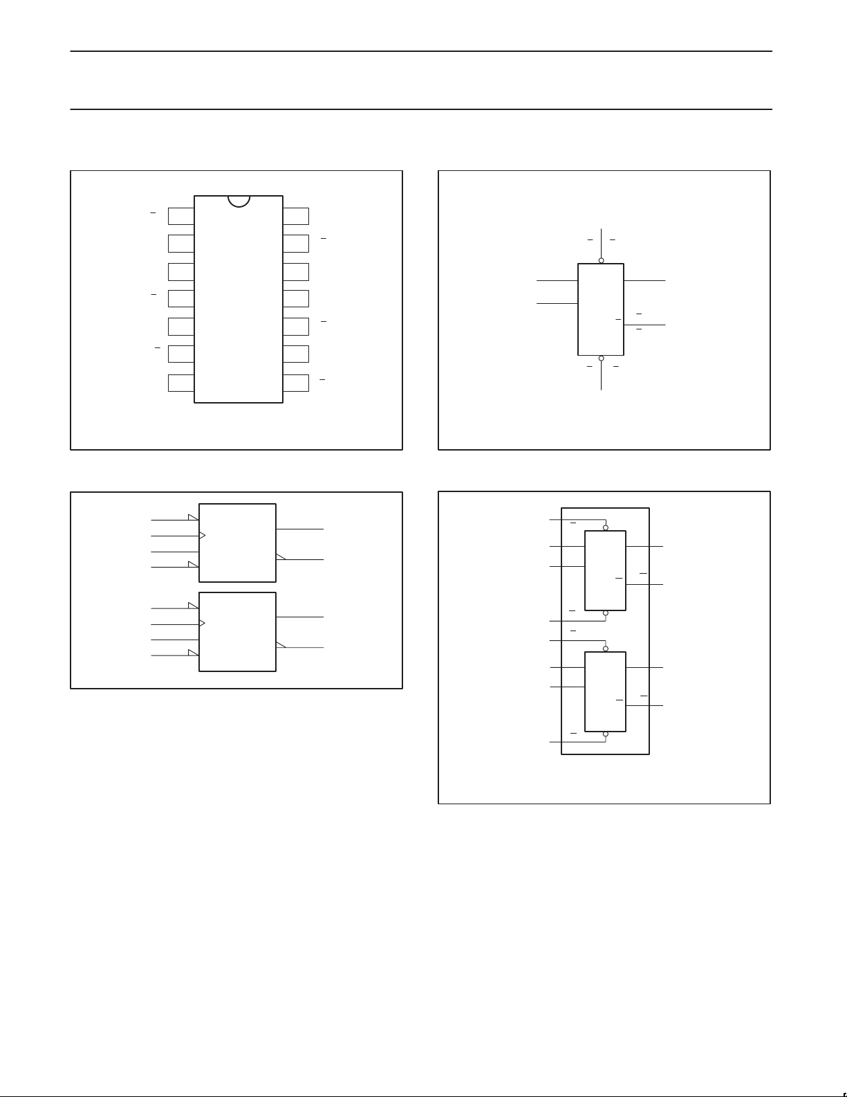
PIN CONFIGURATION
1R
1D
1CP
1S
1Q
1Q
GND
1
D
2
3
4
D
5
6
7
14
13
12
11
10
9
8
SV00330
V
2R
2D
2CP
2S
2Q
2Q
CC
D
D
LOGIC SYMBOL
10
4
2S
1S
D
D
S
21D 1Q 5
12 2D 2Q 9
3 1CP
11 2CP
D
D
CP
R
D
1RD2R
113
Q
FF
Q
1Q
2Q 8
D
SV00331
74LV74
6
LOGIC SYMBOL (IEEE/IEC)
4
3
2
1
10
11
12
13
S
C1
1D
R
S
C2
2D
R
SV00332
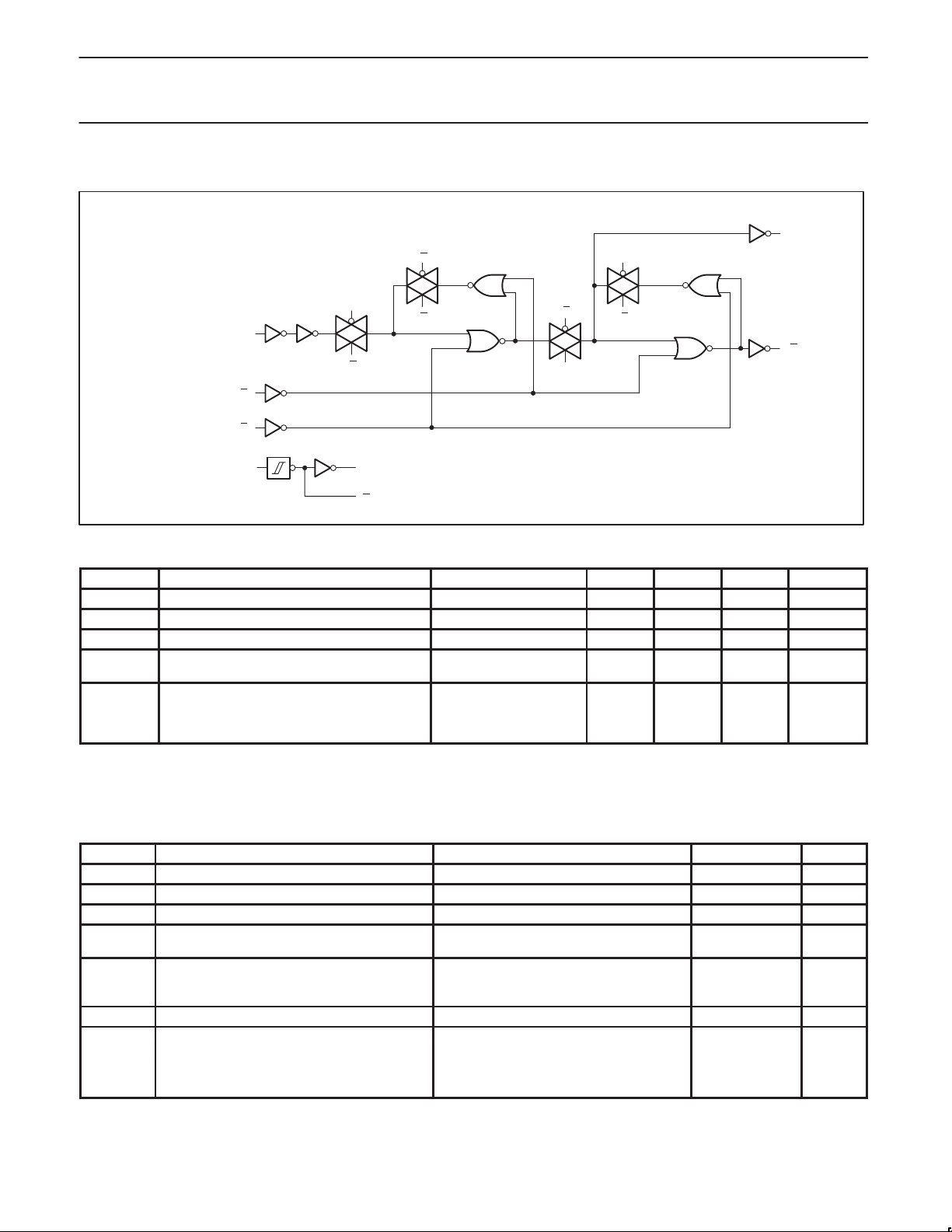
FUNCTIONAL DIAGRAM
5
6
9
8
4
3
1
10
13
1S
1D2
1CP
1R
2S
2D12
2CP11
2R
D
D
D
D
S
D
DQ
CP FF1
Q
R
D
S
D
DQ
CP FF2
Q
R
D
SV00333
1Q
1Q
2Q 9
2
Q
5
6
8
1998 Apr 20
3
Philips Semiconductors Product specification
P
mW
Dual D-type flip-flop with set and reset;
positive edge-trigger
LOGIC DIAGRAM (ONE FLIP-FLOP)
C
CP
C
D
C
R
D
S
D
C
C
C
74LV74
Q
C
C
C
C
Q
SV00334
RECOMMENDED OPERA TING CONDITIONS
SYMBOL PARAMETER CONDITIONS MIN TYP. MAX UNIT
V
CC
V
V
T
amb
tr, t
NOTE:
1. The LV is guaranteed to function down to V
ABSOLUTE MAXIMUM RATINGS
In accordance with the Absolute Maximum Rating System (IEC 134)
Voltages are referenced to GND (ground = 0V)
SYMBOL
V
CC
±I
IK
±I
OK
±I
O
±I
GND
±I
CC
T
stg
tot
NOTES:
1. Stresses beyond those listed may cause permanent damage to the device. These are stress ratings only and functional operation of the
device at these or any other conditions beyond those indicated under “recommended operating conditions” is not implied. Exposure to
absolute-maximum-rated conditions for extended periods may affect device reliability .
2. The input and output voltage ratings may be exceeded if the input and output current ratings are observed.
DC supply voltage See Note1 1.0 3.3 5.5 V
Input voltage 0 – V
I
Output voltage 0 – V
O
Operating ambient temperature range in free
air
Input rise and fall times except for
f
Schmitt-trigger inputs
= 1.0V (input levels GND or VCC); DC characteristics are guaranteed from VCC = 1.2V to VCC = 5.5V.
CC
See DC and AC
characteristics
VCC = 1.0V to 2.0V
V
= 2.0V to 2.7V
CC
VCC = 2.7V to 3.6V
VCC = 3.6V to 5.5V
–40
–40
–
–
–
–
+85
+125
–
–
–
500
200
100
–
1, 2
PARAMETER CONDITIONS RATING UNIT
DC supply voltage –0.5 to +7.0 V
DC input diode current VI < –0.5 or VI > VCC + 0.5V 20 mA
DC output diode current VO < –0.5 or VO > VCC + 0.5V 50 mA
DC output source or sink current
– standard outputs
DC VCC or GND current for types with
,
–standard outputs 50
–0.5V < VO < VCC + 0.5V
25
Storage temperature range –65 to +150 °C
Power dissipation per package for temperature range: –40 to +125°C
–plastic DIL above +70°C derate linearly with 12mW/K 750
–plastic mini-pack (SO) above +70°C derate linearly with 8 mW/K 500
–plastic shrink mini-pack (SSOP and TSSOP) above +60°C derate linearly with 5.5 mW/K 400
50
CC
CC
V
V
°C
ns/V
mA
mA
1998 Apr 20
4
 Loading...