

Philips 74lv688 DATASHEETS
INTEGRATED CIRCUITS
74LV688
8-bit magnitude comparator
Product specification
Supersedes data of 1997 May 15
IC24 Data Handbook
1998 Jun 23
Philips Semiconductors Product specification
74L V6888-bit magnitude comparator
FEA TURES
•Wide operating voltage: 1.0 to 5.5V
•Optimized for low voltage applications: 1.0V to 3.6V
•Accepts TTL input levels between V
•Typical V
T
amb
•Typical V
T
amb
(output ground bounce) < 0.8V at VCC = 3.3V,
OLP
= 25°C
(output VOH undershoot) > 2V at VCC = 3.3V,
OHV
=25°C
= 2.7V and VCC = 3.6V
CC
DESCRIPTION
The 74LV688 is a high-speed Si-gate CMOS device, pin compatible
with the 74HC/HCT688
The 74LV688 is an 8-bit magnitude comparator. It performs
comparisons of two 8-bit binary or BCD words. The output provides
P = Q
(equal-to).
•Compare two 8-bit words
•Output capability: standard
•I
category: MSI
CC
QUICK REFERENCE DATA
SYMBOL PARAMETER CONDITIONS TYPICAL UNIT
t
PHL/tPLH
C
I
C
PD
Propagation delay Pn, Qn to P=Q
Input capacitance 3.5 pF
Power dissipation capacitance per gate VI = GND to V
NOTE:
is used to determine the dynamic power dissipation (PD in W):
1. C
PD
= CPD × V
P
D
f
= input frequency in MHz; CL = output load capacity in pF;
i
= output frequency in MHz; VCC = supply voltage in V;
f
o
× V
(C
L
2
× fi + (CL × V
CC
2
× fo) = sum of outputs.
CC
2
× fo) where:
CC
CL = 15pF
VCC = 3.3V
CC
17 ns
1
22 pF
ORDERING INFORMATION
PACKAGES TEMPERATURE RANGE OUTSIDE NORTH AMERICA NORTH AMERICA PKG. DWG. #
20-Pin Plastic DIL –40°C to +125°C 74LV688 N 74LV688 N SOT146-1
20-Pin Plastic SO –40°C to +125°C 74LV688 D 74LV688 D SOT163-1
20-Pin Plastic SSOP Type II –40°C to +125°C 74LV688 DB 74LV688 DB SOT339-1
20-Pin Plastic TSSOP Type I –40°C to +125°C 74LV688 PW 74LV688PW DH SOT360-1
PIN CONFIGURATION
1
2
P0
3
Q0
4
P1
5
Q1
6
P2
7
Q2
8
P3
9
Q3
GND
20E
19
18
17
16
15
14
13
12
1110
SY00054
V
CC
P = Q
Q7
P7
Q6
P6
Q5
P5
Q4
P4
PIN DESCRIPTION
PIN NO. SYMBOL FUNCTION
1 E Enable input (active LOW)
2, 4, 6, 8, 11,
13, 15, 17
3, 5, 7, 9, 12,
14, 16, 18
10 GND Ground (0V)
19 P=Q Equal to output
20 V
P0 to P7 Word inputs
Q0 to Q7 Word inputs
CC
Positive Supply Voltage
1998 Jun 23 853-1878 19618
2
Philips Semiconductors Product specification
74LV6888-bit magnitude comparator
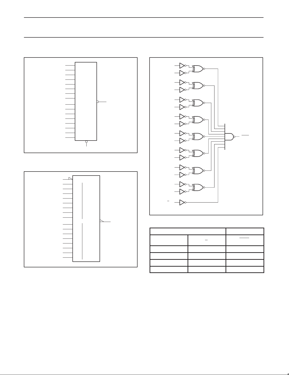
LOGIC SYMBOL
2
4
6
8
11
13
15
17
3
5
7
9
12
14
16
18
P0
P1
P2
P3
P4
P5
P6
P7
Q0
Q1
Q2
Q3
Q4
Q5
Q6
Q7
LOGIC SYMBOL (IEEE/IEC)
1
2
4
6
8
11
13
15
17
3
5
7
9
12
14
16
18
G1
0
7
0
7
E
1
P
(P = Q) 1
Q
SY00055
SY00056
LOGIC DIAGRAM
P7
Q7
P6
Q6
19P = Q
19
P5
Q5
P4
Q4
P3
Q3
P2
Q2
P1
Q1
P0
Q0
E
P = Q
SY00057
FUNCTION TABLE
INPUTS OUTPUT
DATA
Pn, Qn
P = Q L L
X H H
P > Q L H
P < Q L H
NOTES:
H = HIGH voltage level
L = LOW voltage level
X = Don’t care
ENABLE
E
P = Q
1998 Jun 23
3
Philips Semiconductors Product specification
SYMBOL
PARAMETER
CONDITIONS
MIN.TYP.MAX.UNIT
74LV6888-bit magnitude comparator
ABSOLUTE MAXIMUM RATINGS
1, 2
In accordance with the Absolute Maximum Rating System (IEC 134).
Voltages are referenced to GND (ground = 0V).
SYMBOL
V
CC
I
IK
I
OK
I
O
± I
GND,
± I
CC
T
stg
P
tot
DC supply voltage –0.5 +7.0 V
DC input diode current VI < –0.5 V or V1 > VCC + 0.5V – ± 20 mA
DC output diode current VO < –0.5 V or V0 > VCC + 0.5V – ± 50 mA
DC output source or sink current
– standard outputs
DC VCC or GND current for types with
– standard outputs
Storage temperature range –65 +150 °C
power dissipation per package
– plastic DIL
– plastic mini-pack (SO)
– plastic medium-shrink SO (SSOP and TSSOP)
PARAMETER CONDITIONS MIN MAX UNIT
–0.5V < VO < VCC +0.5V ± 25
± 50
for temperature range: –40 to +125°C
above +70°C derate linearly with 12 mW/K
above +70°C derate linearly with 8 mW/K
above +60°C derate linearly with 5.5 mW/K
–
–
–
750
500
400
mW
NOTES:
1. Stresses beyond those listed may cause permanent damage to the device. These are stress ratings only and functional operation of the
device at these or any other conditions beyond those indicated under “recommended operating conditions” is not implied. Exposure to
absolute–maximum–rated conditions for extended periods may affect device reliability .
2. The performance capability of a high–performance integrated circuit in conjunction with its thermal environment can create junction
temperatures which are detrimental to reliability. The maximum junction temperature of this integrated circuit should not exceed 150°C.
3. The input and output negative voltage ratings may be exceeded if the input and output clamp current ratings are observed.
mA
mA
RECOMMENDED OPERATING CONDITIONS
V
V
V
T
amb
tr, t
∆t/∆v)
(
NOTE:
1. The LV is guaranteed to function down to V
DC supply voltage see note 1 1.0 3.3 5.5 V
CC
DC Input voltage 0 – V
I
DC output voltage 0 – V
O
Operating ambient temperature range in
free–air
f
Input rise and fall times
= 1.0V (input levels GND or VCC); DC characteristics are guaranteed from VCC = 1.2V to VCC = 5.5V.
CC
See DC and AC characteristics –40
–40
VCC = 1.0V to 2.0V
VCC = 2.0V to 2.7V
VCC = 2.7V to 3.6V
V
= 3.6V to 5.5V
CC
CC
CC
–
–
–
–
–
–
+85
+125
500
200
100
50
V
V
°C
ns/V
1998 Jun 23
4
 Loading...