

Philips 74LV595PW, 74LV595N, 74LV595DB, 74LV595D Datasheet

INTEGRATED CIRCUITS
74LV595
8-bit serial-in/serial or parallel-out shift
register with output latches (3-State)
Product specification 1998 Apr 20
IC24 Data Handbook
Philips Semiconductors Product specification
8-bit serial-in/serial or parallel-out shift register
with output latches (3-State)
FEA TURES
•Optimized for Low Voltage applications: 1.0V to 3.6V
•Accepts TTL input levels between V
•Typical V
T
amb
•Typical V
T
amb
(output ground bounce) < 0.8V at V
OLP
= 25°C
(output VOH undershoot) > 2V at V
OHV
= 25°C
= 2.7V and V
CC
CC
CC
CC
= 3.3V ,
= 3.3V ,
•8-bit serial input
•8-bit serial or parallel output
•Storage register with 3-State outputs
•Shift register with direct clear
•Output capability:
– parallel outputs; bus driver
– serial output; standard
•I
category: MSI
CC
QUICK REFERENCE DATA
GND = 0V; T
SYMBOL
t
PHL/tPLH
f
max
C
I
C
PD
NOTES:
is used to determine the dynamic power dissipation (PD in µW)
1. C
PD
P
= CPD V
D
= input frequency in MHz; CL = output load capacitance in pF;
f
i
f
= output frequency in MHz; VCC = supply voltage in V;
o
(C
2. The condition is V
= 25°C; tr =tf 2.5 ns
amb
CC
2
V
L
fo) = sum of the outputs.
CC
PARAMETER CONDITIONS TYPICAL UNIT
Propagation delay
SHCP to Q
STCP to Q
MR to Q
Maximum clock frequency SHCP, ST
Input capacitance 3.5 pF
Power dissipation capacitance per gate
2
x fi (CL V
= GND to V
I
7’
CC.
7’
7’
CC
2
fo) where:
= 3.6V
CP
APPLICATIONS
•Serial-to-parallel data conversion
•Remote control holding register
DESCRIPTION
The 74LV595 is a low-voltage Si-gate CMOS device that is pin and
function compatible with 74HC/HCT595.
The74L V595 is an 8-stage serial shift register with a storage register
and 3-State outputs. The shift register and storage register have
separate clocks.
Data is shifted on the positive-going transitions of the SH
The data in each register is transferred to the storage register on a
positive-going transition of the ST
connected together , the shift register will always be one clock pulse
ahead of the storage register.
The shift register has a serial input (D
(Q
) all for cascading. It is also provided with asynchronous reset
7’
(active LOW) for all 8 shift register stages. The storage register has
8 parallel 3-State bus driver outputs. Data in the storage register
appears at the output whenever the output enable input (OE
LOW.
CL = 15pF
VCC= 3.3V 15
VCC = 3.3V
Notes 1 and 2
74L V595
input. If both clocks are
CP
) and a serial standard output
S
16
14
77 MHz
115 pF
CP
input.
) is
ns
ORDERING AND PACKAGE INFORMA TION
PACKAGES TEMPERATURE RANGE OUTSIDE NORTH AMERICA NORTH AMERICA PKG. DWG. #
16-Pin Plastic DIL –40°C to +125°C 74LV595 N 74LV595 N SOT38-4
16-Pin Plastic SO –40°C to +125°C 74LV595 D 74LV595 D SOT109-1
16-Pin Plastic SSOP Type II –40°C to +125°C 74LV595 DB 74LV595 DB SOT338-1
16-Pin Plastic TSSOP Type I –40°C to +125°C 74L V595 PW 74LV595PW DH SOT403-1
1998 Apr 20 853-1987 19255
2
Philips Semiconductors Product specification
FUNCTION
8-bit serial-in/serial or parallel-out shift register
with output latches (3-State)
PIN DESCRIPTION
PIN
NUMBER
15, 1, 2, 3,
4, 5, 6, 7
8 GND Ground (0V)
9 Q
10 MR Master reset (active LOW)
11 SH
12 ST
13 OE Output enable input (active LOW)
14 D
16 V
SYMBOL FUNCTION
Q0 to Q7Parallel data output
Serial data output
7’
Shift register clock input
CP
Storage register clock input
CP
Serial data input
S
Positive supply voltage
CC
FUNCTION TABLE
INPUTS OUTPUTS
SH
H = HIGH voltage level
L = LOW voltage level
X = Don’t care
Z = High impedance OFF-state
NC= No change
= LOW-to-HIGH clock transition
↓ = HIGH-to-LOW transition
CP
ST
OE MR D
CP
S
Q
7’
Qn
X X L L X L NC A LOW level on MR only affects the shift registers
X L L X L L Empty shift register loaded into storage register
X X H L X L Z Shift register clear. Parallel outputs in high-impedance OFF-states
X L H H Q
6’
X L H X NC Q
L H X Q
6’
NC
Q
n’
n’
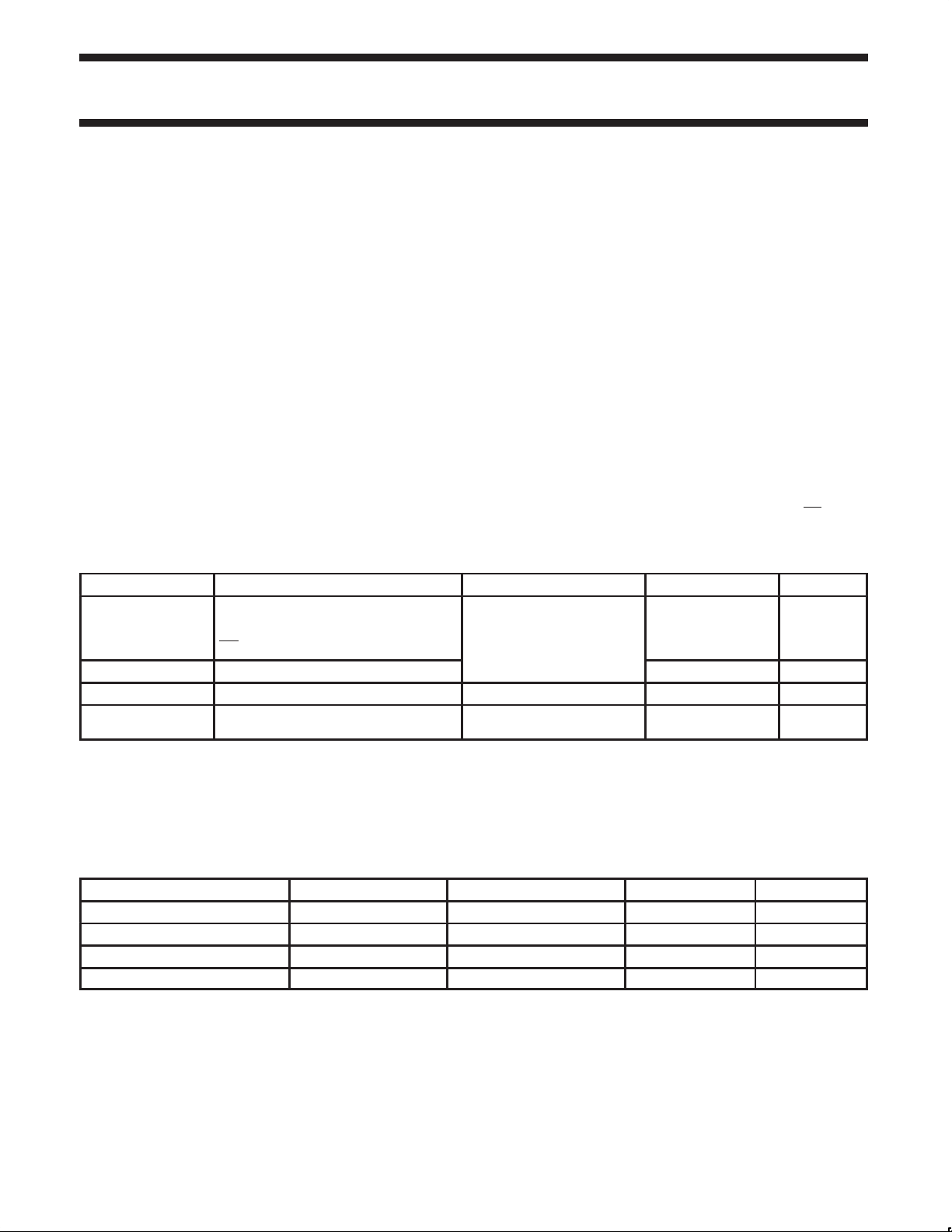
PIN CONFIGURATION
Q
1
1
Q
2
2
Q
3
3
Q
4
4
Q
5
5
Q
6
6
Q
7
7
GND
8
Logic high level shifted into shift register stage 0. Contents of all shift
register stages shifted through, e.g. previous state of stage 6 (internal
Q
) appears on the serial output (Q7’)
6’
Contents of shift register stages (internal Qn’) are transferred to the
storage register and parallel output stages
Contents of shift register shifted through. Previous contents of the shift
register are transferred to the storage register and the parallel output
stages
16
15
14
13
12
11
10
9
SV00720
74LV595
V
CC
Q
0
D
S
OE
ST
CP
SH
CP
MR
Q
7’
1998 Apr 20
3
Philips Semiconductors Product specification
8-bit serial-in/serial or parallel-out shift register
with output latches (3-State)
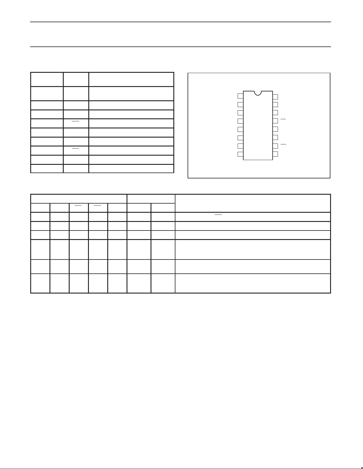
LOGIC SYMBOL
14
11
SH
CP
D
S
MR OE
12
ST
CP
Q
7’
Q
0
Q
1
Q
2
Q
3
Q
4
Q
5
Q
6
Q
7
9
15
1
2
3
4
5
6
7
FUNCTIONAL DIAGRAM
74LV595
D
S
14
SH
CP
11
MR
10
ST
CP
12
OE
13
Q0Q1Q2Q3Q4Q5Q6Q
15 1 2 3 4 5 6 7
8–STAGE SHIFT
REGISTER
8–BIT STORAGE
REGISTER
3–STATE OUTPUTS
Q7’
9
7
10 13
LOGIC SYMBOL (IEEE/IEC)
13
12
10
11
14
SRG8
R
C1/
1D
EN3
2D
SV00723
C2
3
15
1
2
3
4
5
6
7
9
SV00724
SV00725
1998 Apr 20
4

Philips Semiconductors Product specification
8-bit serial-in/serial or parallel-out shift register
with output latches (3-State)
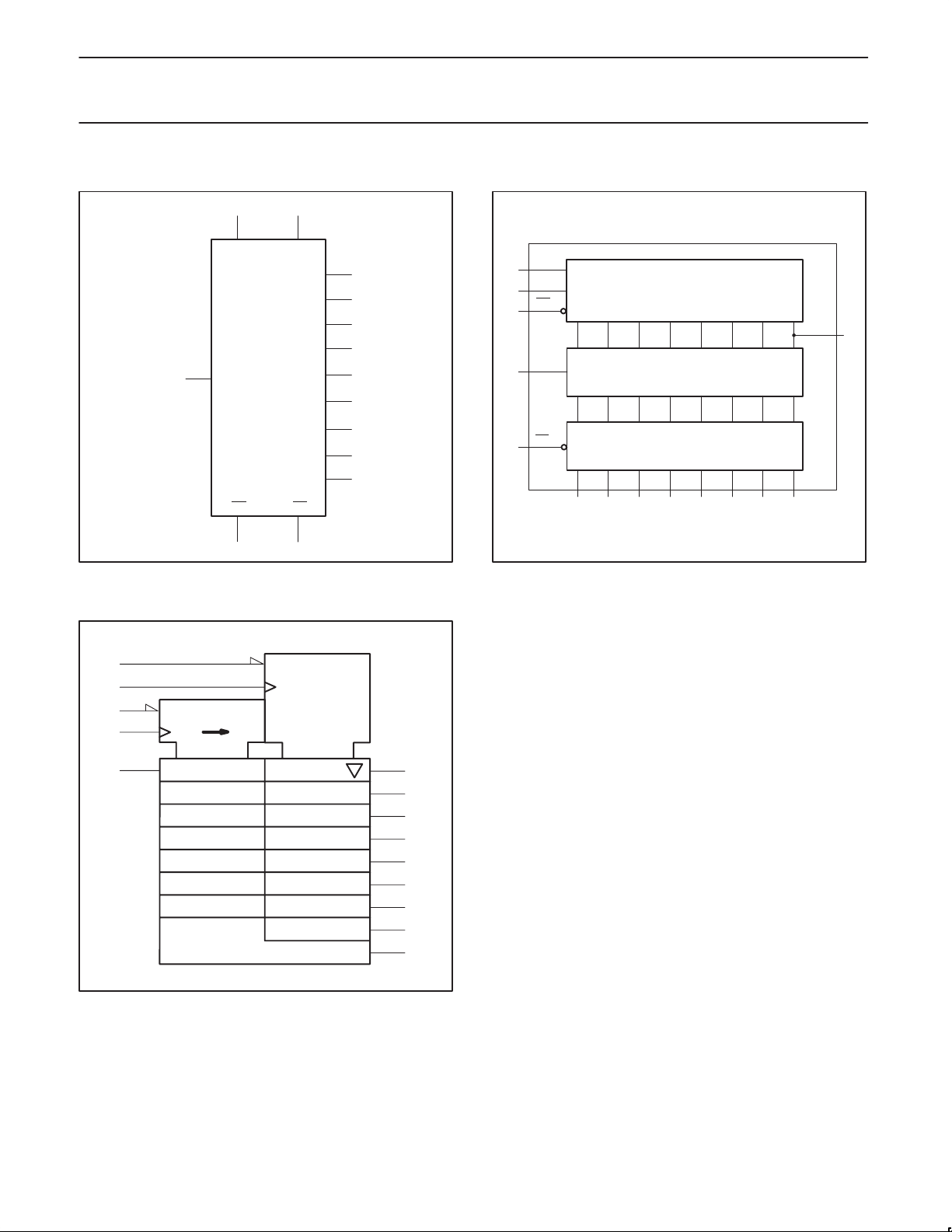
LOGIC DIAGRAM
SH
STAGE 0 STAGE 7
D
S
CP
MR
ST
CP
OE
D
FFO
CP
R
D
LATCH
CP
Q
Q
STAGES 1 to 6
DQ
D
FF7
CP
R
D
LATCH
CP
74LV595
Q
Q
Q7’
TIMING DIAGRAM
SHCP
DS
STCP
MR
OE
Q0
Q1
Q6
Q
0
Q1Q2Q3Q4Q5Q
6
Z–state
Z–state
Z–state
Q
7
SV00721
1998 Apr 20
Q7’
Q7
Z–state
SV00726
5
 Loading...