

Philips 74lv541 DATASHEETS
INTEGRATED CIRCUITS
74LV541
Octal buffer/line driver (3-State)
Product specification
Supersedes data of 1997 Mar 04
IC24 Data Handbook
1997 Jun 10
Philips Semiconductors Product specification
74L V541Octal buffer/line driver (3-State)
FEA TURES
•Optimized for Low Voltage applications: 1.0 to 3.6V
•Accepts TTL input levels between V
•Typical V
T
amb
•Typical V
T
amb
(output ground bounce) 0.8V @ VCC = 3.3V,
OLP
= 25°C
(output VOH undershoot) 2V @ VCC = 3.3V,
OHV
= 25°C
= 2.7V and VCC = 3.6V
CC
•Non-inverting outputs
•Output capability: bus driver
•I
category: MSI
CC
QUICK REFERENCE DATA
GND = 0V; T
SYMBOL
t
PHL/tPLH
C
I
C
PD
NOTES:
is used to determine the dynamic power dissipation (PD in µW)
1. C
PD
P
= CPD V
D
= input frequency in MHz; CL = output load capacity in pF;
f
i
f
= output frequency in MHz; VCC = supply voltage in V;
o
(C
= 25°C; tr = tf 2.5 ns
amb
CC
2
V
L
fo) = sum of the outputs.
CC
PARAMETER CONDITIONS TYPICAL UNIT
Propagation delay
An to Y
n
Input capacitance 3.5 pF
Power dissipation capacitance per buffer VI = GND to VCC
2
fi (CL V
2
fo) where:
CC
DESCRIPTION
The 74LV541 is a low–voltage CMOS device and is pin and function
compatible with 74HC/HCT541.
The 74LV541 is an octal non-inverting buf fer/line driver with 3-State
outputs. The 3-State outputs are controlled by the output enable
inputs OE
A HIGH on OEn causes the outputs to assume a high impedance
OFF–state.
CL = 15pF
VCC = 3.3V
and OE2.
1
1
10 ns
37 pF
ORDERING INFORMATION
PACKAGES TEMPERATURE RANGE OUTSIDE NORTH AMERICA NORTH AMERICA PKG. DWG. #
20-Pin Plastic DIL –40°C to +125°C 74LV541 N 74LV541 N SOT146-1
20-Pin Plastic SO –40°C to +125°C 74LV541 D 74L541 D SOT163-1
20-Pin Plastic SSOP Type II –40°C to +125°C 74LV541 DB 74LV541 DB SOT339-1
20-Pin Plastic TSSOP Type I –40°C to +125°C 74LV541 PW 74LV541PW DH SOT360-1
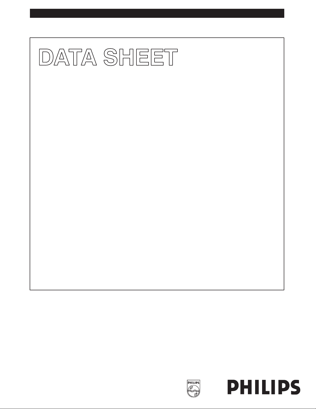
PIN DESCRIPTION
PIN
NUMBER
1, 19 OE1, OE2Output enable input (active-LOW)
2, 3, 4, 5,
6, 7, 8, 9
10 GND Ground (0V)
18, 17, 16, 15,
14, 13, 12, 11
20 V
SYMBOL FUNCTION
A0 to A7Data inputs
Y0 to Y7Bus outputs
CC
Positive supply voltage
FUNCTION TABLE
INPUTS OUTPUT
OE
L L L L
L L H H
X H X Z
H X X Z
H = HIGH voltage level
L = LOW voltage level
X = Don’t care
Z = High impedance OFF-state
OE
1
nA nY
2
1998 Jun 10 853–1937 19545
2
Philips Semiconductors Product specification
74LV541Octal buffer/line driver (3-State)
PIN CONFIGURATION
1
OE
1
A
2
0
3
A
1
4
A
2
5
A
3
6
A
4
A
7
5
8
A
6
9
A
7
10
GND
LOGIC SYMBOL
A
2
A
3
A
4
LOGIC SYMBOL (IEEE/IEC)
20
19
18
17
16
15
14
13
12
11
SV00680
V
OE
Y
Y
Y
Y
Y
Y
Y
Y
1
CC
2
0
1
2
3
4
5
6
7
19
2
3
4
5
6
7
8
9
&
EN
18
17
16
15
14
13
12
11
SV00682
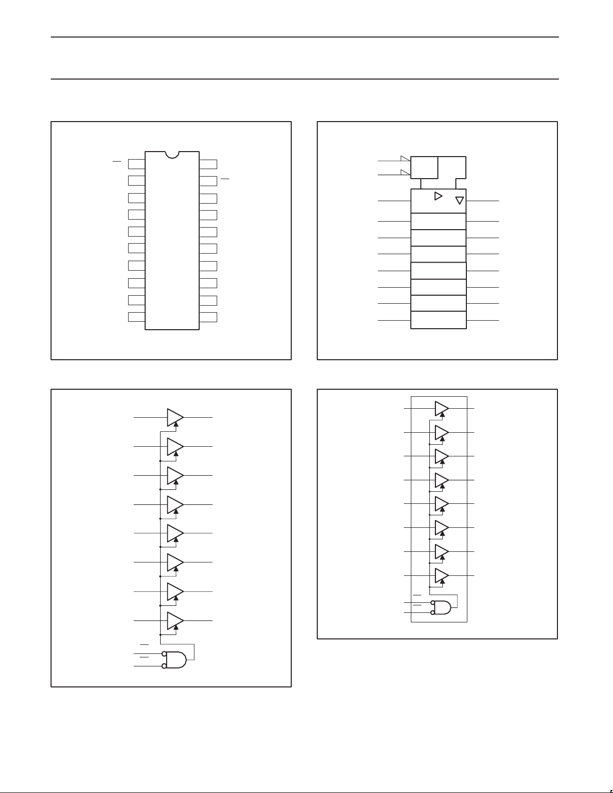
FUNCTIONAL DIAGRAM
A
0
0
1
2
Y
0
18
Y
1
17
Y
2
16
2
A
1
3
A
2
4
A
3
5
Y
0
18
Y
1
17
Y
2
16
Y
3
15
1998 Jun 10
A
3
5
A
4
6
A
5
7
A
6
8
A
7
9
Y
3
15
Y
4
14
Y
5
13
Y
6
12
Y
7
11
A
4
6
A
5
7
A
6
8
A
7
9
OE
1
1
OE
2
19
Y
4
14
Y
5
13
Y
6
12
Y
7
11
SV00683
OE
1
1
OE
2
19
SV00681
3
Philips Semiconductors Product specification
P
mW
74LV541Octal buffer/line driver (3-State)
RECOMMENDED OPERATING CONDITIONS
SYMBOL PARAMETER CONDITIONS MIN TYP MAX UNIT
V
V
V
T
amb
tr, t
NOTE:
1. The LV is guaranteed to function down to V
DC supply voltage See Note 1 1.0 3.3 3.6 V
CC
Input voltage 0 – V
I
Output voltage 0 – V
O
Operating ambient temperature range in free air
Input rise and fall times
f
CC
See DC and AC
characteristics
VCC = 1.0V to 2.0V
VCC = 2.0V to 2.7V
V
= 2.7V to 3.6V
CC
= 1.0V (input levels GND or VCC); DC characteristics are guaranteed from VCC = 1.2V to VCC = 3.6V.
–40
–40
–
–
–
–
–
–
–
CC
CC
+85
+125
500
200
100
V
V
°C
ns/V
ABSOLUTE MAXIMUM RATINGS
1, 2
In accordance with the Absolute Maximum Rating System (IEC 134).
Voltages are referenced to GND (ground = 0V).
SYMBOL
V
CC
±I
IK
±I
OK
±I
O
±I
GND
±I
CC
T
stg
DC supply voltage –0.5 to +4.6 V
DC input diode current VI < –0.5 or VI > VCC + 0.5V 20 mA
DC output diode current VO < –0.5 or VO > VCC + 0.5V 50 mA
DC output source or sink current
– bus driver outputs
DC VCC or GND current for types with
,
–bus driver outputs
Storage temperature range –65 to +150 °C
PARAMETER CONDITIONS RATING UNIT
–0.5V < VO < VCC + 0.5V 35 mA
70 mA
Power dissipation per package for temperature range: –40 to +125°C
–plastic DIL above +70°C derate linearly with 12mW/K 750
tot
–plastic mini-pack (SO) above +70°C derate linearly with 8 mW/K 500
–plastic shrink mini-pack (SSOP and TSSOP) above +60°C derate linearly with 5.5 mW/K 400
NOTES:
1. Stresses beyond those listed may cause permanent damage to the device. These are stress ratings only and functional operation of the
device at these or any other conditions beyond those indicated under “recommended operating conditions” is not implied. Exposure to
absolute-maximum-rated conditions for extended periods may affect device reliability .
2. The input and output voltage ratings may be exceeded if the input and output current ratings are observed.
1998 Jun 10
4
 Loading...